Choosing the optimal materials and fabrication techniques for microfluidic chip and tubing
Writer
Celeste Chidiac, PhD
Keywords
Microfluidic Devices, Intelligent Microfluidics, Artificial Intelligence, Machine Learning
Author
Celeste Chidiac, PhD & Diana Kafizova
Publication Date
Keywords
Intelligent Microfluidics
Deep Learning
Microfluidic Devices
Artificial Intelligence
Machine Learning
PDMS
Thermoplastics
Soft lithography
3D printing
Thermoplastics bonding
Composite materials
Need advice for your fabrication techniques?
Your microfluidic SME partner for Horizon Europe
We take care of microfluidic engineering, work on valorization and optimize the proposal with you
Introduction
In recent decades, microfluidics has emerged as a technological toolset for precision control and fluid monitoring at the microscale. Microfluidics centers around a microfluidics device (or “chip”) containing microchannels [1]. In research, microfluidics device versatility and performance are prioritized, whereas in commercialization, production cost, reliability, and ease of use are placed above all.
The choice of the material can affect its properties, such as absorptivity, permeability, wettability, and biocompatibility. Notably, some unique phenomena occur at the microscale, impacting these properties. For instance, a small mass/heat travel distance will lead to a shorter reaction time; a great surface/volume ratio will lead to greater capillary forces. Therefore, choosing the material is the first and crucial step in microfluidic chip fabrication [2].
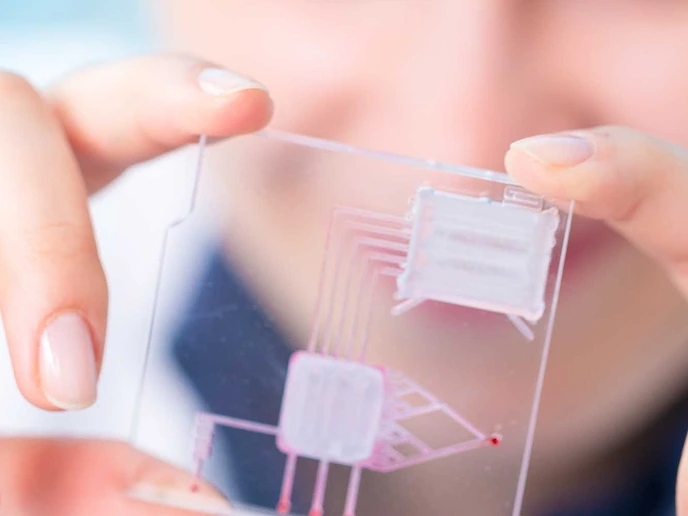
This step is followed by selecting the appropriate chip fabrication and bonding techniques, significantly impacting the microfluidic chip’s functionality, fluid dynamics, and overall cost.
This review will give us an overview of the different materials used in manufacturing microfluidic chips and tubings and the main fabrication and bonding techniques.
Microfluidic tubing fabrication materials
Tubing material (Figure 14) should be selected according to the nature of the reagents flowing through it to prevent interference. Biological and chemical compatibility, inertness, and solvent resistance are important factors to consider. Chemical resistance is particularly critical when working with aggressive solvents or reactive reagents to prevent tubing degradation or alteration of experimental results.
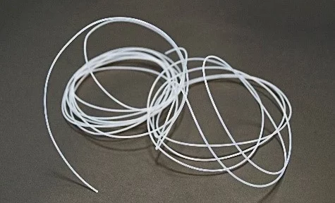
The most common materials for tubing fabrication are polyetheretherketone (PEEK) and perfluorinated polymers.
Polyetheretherketone (PEEK)
Due to its remarkable chemical resistance, PEEK is widely described as the highest-performing thermoplastic material for tubing fabrication. Moreover, PEEK tubing has low non-specific adsorption, is flexible, offers a smooth internal surface, and can be easily cut to desired lengths. This material can be used for low and high-pressure applications.
Perfluorinated polymers
Polytetrafluoroethylene (PTFE), equivalent to the brand name Teflon®. It is chemically inert to most commonly used solvents, non-toxic, non-porous, and has excellent stress- and temperature- resistance. Due to its high flexibility, it is mostly used for low-pressure applications.
Fluorinated ethylene-propylene (FEP), used as an alternative to PTFE, exhibits similar characteristics, such as biocompatibility and chemical inertia to most solvents. It is a flexible material with very good optical properties and is mostly used for low-pressure applications.
Ethylene tetrafluoroethylene (ETFE) is more rigid and chemically resistant than PTFE and FEP, making it better suited to higher-pressure applications.
Microfluidic chip fabrication materials
Various material properties, such as optical, mechanical, gas permeability, and surface wettability, determine its suitability for a specific application. Recent research efforts have been directed toward optimizing the choice of materials.
Glass and silicone are first-generation microfluidic chip materials that are great for capillary electrophoresis but expensive for fabrication. Elastomers allow low-cost rapid prototyping and can generate complex and parallel fluid control. Thermoplastics are a good alternative for elastomers having low cost and rapid fabrication. Paper is a relatively recent material, and it has been widely used for microfluidic device fabrication due to its low price and simplicity [2].
Table 1 summarizes the advantages, limitations, and applications of silicon, glass, polydimethylsiloxane (PDMS), thermoplastics, and paper in microfluidic chip fabrication.
Material
| Advantages | Limitations | Applications |
| Silicon | -Excellent for precise microfabrication -Compatible with micro-electromechanical system (MEMS) devices -High mechanical strength and thermal stability | -Opaque, not suitable for optical detection -Expensive fabrication (photolithography) -Brittle and prone to breaking | -MEMS integration -High-performance applications -Biosensing |
| Glass | -Excellent chemical resistance -High optical clarity for microscopy -Compatible with a wide range of solvents | -Brittle, prone to breakage -Expensive fabrication (etching, bonding) -Requires specialized equipment | – Chemical analysis -Cell culture -Diagnostics with optical detection -Capillary electrophoresis |
| PDMS | -Easy to fabricate with soft lithography -Ideal for rapid prototyping -Optically transparent | -Poor chemical resistance to organic solvents -Prone to deformation at high pressure | -Cell culture -Prototyping -Low-cost bioassays |
| Thermoplastics | -Suitable for mass production -Good mechanical stability -Low-cost fabrication (injection molding, embossing) | -Requires expensive molds for production -Limited flexibility compared to PDMS -Some plastics have high autofluorescence | -Disposable diagnostics -Point-of-care device -Mass-produced lab-on-a-chip systems |
| Paper | -Extremely low-cost fabrication -Capillary action drives fluid flow (no external pumps) -Environmentally friendly, disposable | -Limited mechanical strength -Low flow control -Not compatible with all chemicals | -Point-of-care diagnostics -Environmental monitoring -Simple bioassays |
Let’s have a deeper look at each of these material’s advantages and limitations.
Inorganic materials
Over the last three decades, microfluidics platforms have revolutionized fluidic automation, biochemical assays, high-throughput clinical screening, and other areas [3]. Early microfluidics was based on fabricating devices on silicon wafers using photolithography and subsequent wet etching, or micromachining. These techniques were adapted to glass substrates for more favorable optical properties and suitable conductivity for electro-osmotic flow.
Silicon
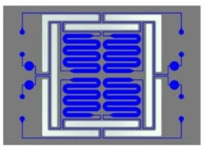
For decades, silicon was among the first choices for microfluidic chip fabrication due to its availability, chemical compatibility, and thermostability (Figure 1). Adding to these are its ease of fabrication, design flexibility, semiconducting properties, and the possibility of surface modifications. The semiconductor properties of silicon have led to its active use in the microfabrication field. However, silicon is opaque, which makes it unsuitable for optical detection.
Moreover, its fragility and high elastic modulus hinder the incorporation of active components, such as valves and pumps, in the silicon platform. Despite these disadvantages and its high price, silicon microfluidic chips are used in point-of-care medical diagnostics and organ-on-chip devices for drug screening [4].
Glass
Glass is an amorphous material, optically transparent and electrically insulating (Figure 2). It has excellent chemical resistance and thermal stability, making it ideal for precise control and durability applications. It is compatible with biological samples, is impermeable to gas, and has relatively low non-specific adsorption [6].
However, the fabrication of microfluidics glass chips is expensive and complex, involving dangerous chemicals that require protective facilities. The bonding of chips is difficult due to the need for high temperature, high pressure, and an extremely clean environment. Thus, glass devices have complications in preloading the reagents before the assembly [4].
One major application of glass chips is capillary electrophoresis (CE). On-chip CE is lower in cost and easier to parallel than standard CE. Due to high thermal conductivity and stable electroosmotic mobility on its surface, glass channels provide better performance [2].
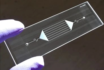
However, the widespread implementation of silicon and glass microfluidics devices has been severely limited by their costly and laborious fabrication process and poor scalability. Thus, to encourage wider adoption of microfluidics, there was a push toward polymeric materials, which require faster, less specialized fabrication techniques.
Polymers
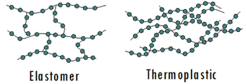
Polymers were introduced in the industry in the 1930s. Since then, elastomers and thermoplastics (Figure 3) have been refined and used to mass-produce high-quality microfluidics devices. For this reason, many microfluidics experts have focused on producing chips with rigid polymers as a bulk material [4].
Elastomers
PDMS
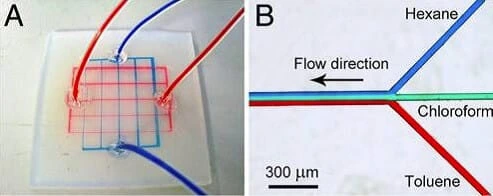
Polydimethylsiloxane (PDMS) has revolutionized microfluidics since its introduction as a microfluidics material in 1998 by George Whitesides’ group at Harvard University [6] (Figure 6). The name poly(dimethyl siloxane) originates from the silicon atom with two methyl groups, and sometimes, instead of a methyl group, there is a link to another backbone. Its backbone is a flexible 3-D chain where each Si-O bond can be symmetrically rotated. More cross-linking leads to more hardness and less elasticity [7].
PDMS has been widely used in microfluidics for rapid prototyping due to its low price, optical transparency, biocompatibility, elastomeric properties, and simplicity of molding and prototyping. In addition, its light transmittance and ability to easily bond with various materials at room temperature attracted much attention.
Microfluidics device molds are formed via conventional machining or photolithography methods [8]. PDMS is mixed with a curing agent and degassed inside a desiccator. Then, the mix is poured over the mold and cured in a conventional oven. Once ready, the chips are demolded and cut, and inlets are pierced with biopsy punchers. Lastly, the PDMS is bound to a glass slide after treatment in a plasma cleaner (Figure 4).

Notably, PDMS microfluidic chips have shown limitations in surface treatment stability, chemical compatibility, and a high tendency for biomolecule adsorption, making them unsuitable for many biomedical applications [9].
Perfluorinated polymers
Fabricating and using perfluorinated polymers (e.g. all-Teflon chips) with high inertness and both oleophobic and hydrophobic surfaces is a good alternative to glass or silicon. Thus, researchers started to figure out how to use solid Teflons directly to accomplish whole-Teflon chip fabrication. Like amorphous Teflons, semi-crystalline solid Teflons are extremely chemically inert, non-sticky, flexible, optically transparent, and can prevent leaching problems with better hardness. In addition, they are soft, show low nonspecific protein adsorption, no evidence of swelling, and high compatibility with all solvents, compared with PDMS [10, 11].
Some researchers also adopted photocurable perfluoropolyethers (PFPEs), fluoropolymers that are liquids at room temperature but solidified after fully curing. PFPE exhibits low surface energy and temperature resistance up to 240 °C, which ensures its ability to fabricate microreactors for organic synthesis. Due to its hydrophobic nature, PFPE is naturally resistant to fouling channel blockage when aqueous solutions are involved [10, 11].
Nevertheless, the difficulty in fabrication and the high cost of the polymer resin limited broad applications. The first whole-Teflon microfluidic chip was made of perfluoroalkoxy (PFA) (An example of a PFA chip is shown in Figure 5). It can be molded by conventional thermoplastic processing methods; it shows excellent mechanical strength, resistance to corrosion, and amenability for cell culture. PFA is slightly opaque but can be employed in fluorescence and cellular imaging. Being used for the fabrication of cheap and reusable microfluidic chips (without contamination risk), PFA requires high-temperature embossing (∼260 °C) to mold devices.
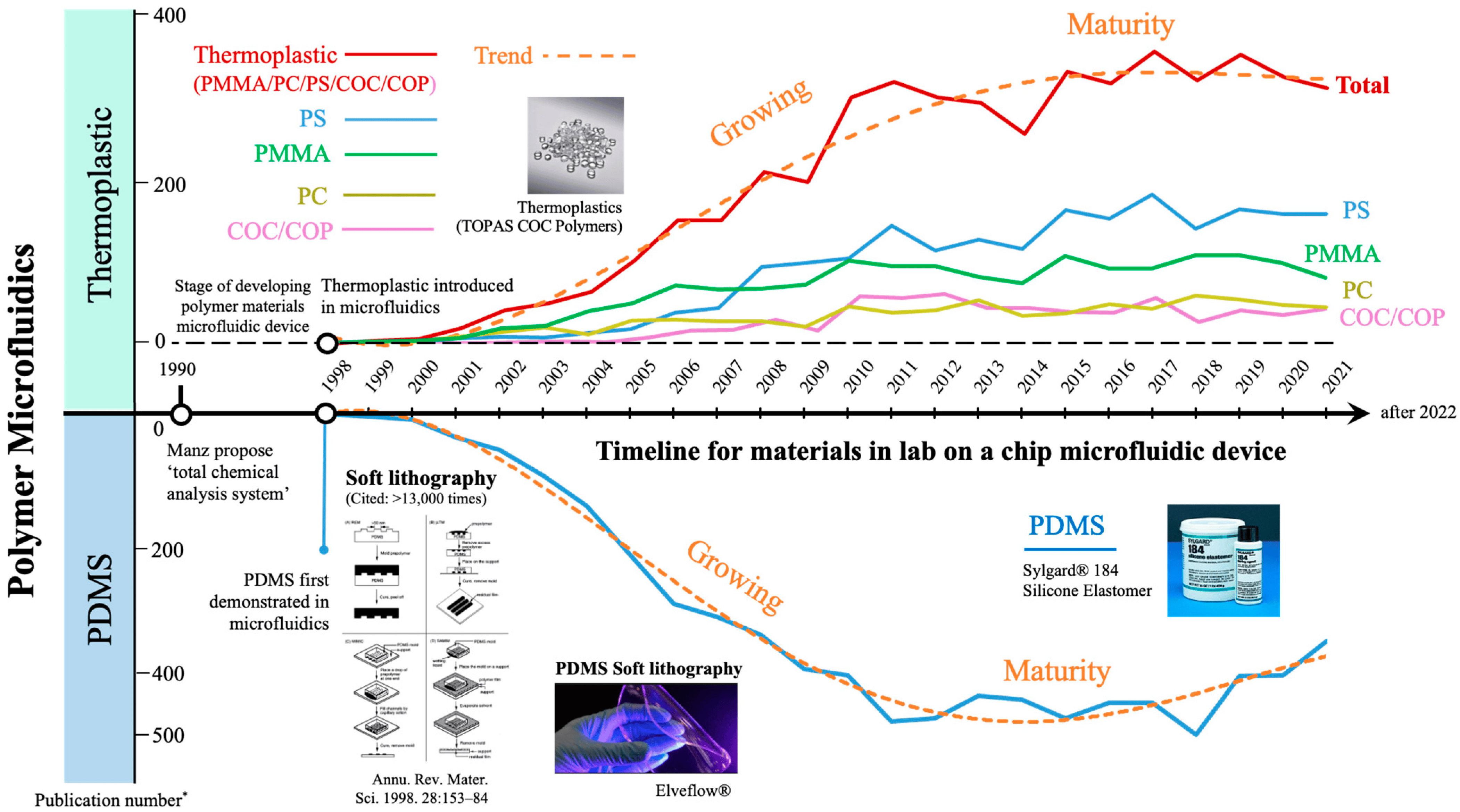
Other polymers, such as thermoplastics, have recently attracted considerable research interest in microfluidics (Figure 6). The main driver for the shift from PDMS to thermoplastics is their streamlined and inexpensive fabrication processes, which make mass production of microfluidics devices easily imaginable.
Thermoplastics
Thermoplastics started gaining popularity in microfluidic chip fabrication in the early 2000s (Figure 6). Thermoplastics are highly crosslinked polymers that can retain their shape after cooling (Figure 3). They are also suitable for micro-machining processes and can be remolded multiple times.
The performance of polymer surfaces in biological environments depends upon the chemical and physical attributes of their surface. Factors such as hydrophilicity/hydrophobicity, chemical structure, roughness, morphology, and surface functional groups significantly influence cell adhesion and proliferation.
Most polymers inherently exhibit hydrophobicity and biological neutrality, making them unsuitable as cell adhesion, coating, and non-cell adhesive substrates without surface modification [14].
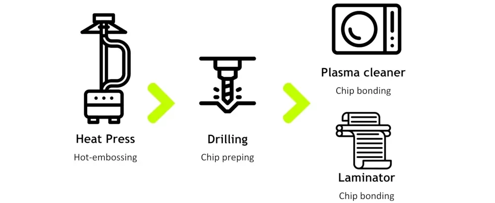
We have developed a thermoplastic molding setup in which the first time-consuming part of the microfabrication process is substituted with a much quicker hot embossing process. Then, the chip prepping can be done with a drilling tool, and the chip bonding can be done with the plasma cleaner and a laminator (Figure 7).
While each thermoplastic’s material properties vary, poly(methyl methacrylate) (PMMA), polystyrene (PS), polycarbonate (PC), cyclic olefin (co)polymer (COC/COP), and polyurethane (PU), offer good optical properties, low gas permeability, relatively stable surface properties, and biocompatibility. In addition, they are resistant to the permeation of small molecules and stiffer than elastomers [13].
Poly-methyl methacrylate (PMMA)
PMMA is the most widely used thermoplastic polymer in microfluidics, especially for fabricating disposable chips, because of its low price, excellent optical transparency, and compatibility with electrophoresis. In addition, PMMA is less hydrophobic than other plastic materials and is biocompatible with high mechanical strength and temperature resistance [3]. However, PMMA has low stability against organic solvents and poor UV transmissivity.
Prepolymers consisting of the monomer MMA and the polymer PMMA were used for high-resolution replication of microfluidic chips from PDMS or stainless steel [10].
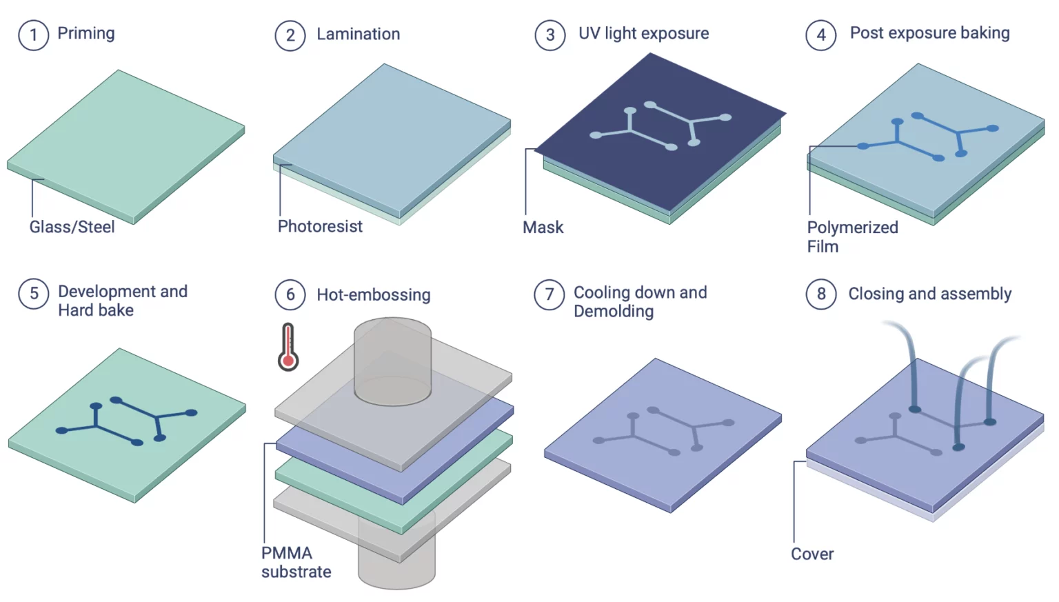
PMMA chips can be fabricated using hot embossing, and PMMA-PMMA substrates sealed using solvent bonding, thermal bonding, or chemical bonding (Figure 6). However, doping and embedding different components into the PMMA structure can modify this polymer’s optical properties [15].
PMMA has been used as a substrate for many microfluidics devices, including mixing analysis chips, DNA sequencers, and electrophoresis chips.
We have developed a PMMA device station for high-resolution PMMA chip fabrication (Figure 8).
Polystyrene (PS)
The use of polystyrene (PS) in chip fabrication is very favorable due to its excellent biocompatibility, transparency, commercial availability, and potential for mass production via techniques such as hot embossing and injection molding. Our thermoplastic molding setup can be used to manufacture PS chips.
Notably, PS is considered a standard non-toxic substrate with mechanical properties suitable for fabricating both animal and human cell/tissue culture chips [14]. PS surface is highly hydrophobic but can be made hydrophilic by various physical and chemical means. However, the necessity of expensive equipment could hinder its use.
In addition, it is possible to modify the PS surface to enhance cell adhesion and interactions between the biomaterial surface and the biological milieu, and prevent bubble formation, all while preserving the material’s bulk properties. To that extent, the material can be treated with oxygen plasma before bonding, which is prone to modification in bond strength, altering the PS surface’s chemical composition. Another method consists of UV irradiating or pre-coating microchannels with extracellular matrix proteins before cell seeding [14].
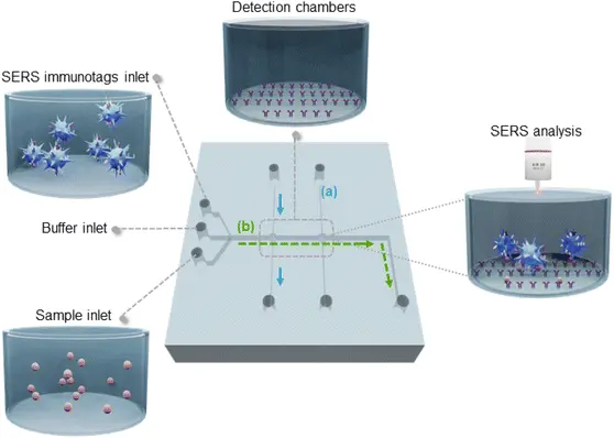
An example of a PS microfluidic chip is shown in Figure 9.
Polycarbonate (PC)
Polycarbonate (PC) has similar characteristics to PMMA, but PC is more expensive, stronger, and has a high-temperature resistance. It is also highly transparent and offers light transmission as good as glass, and is known for its mechanical strength, low density, good biocompatibility, and low moisture absorption.
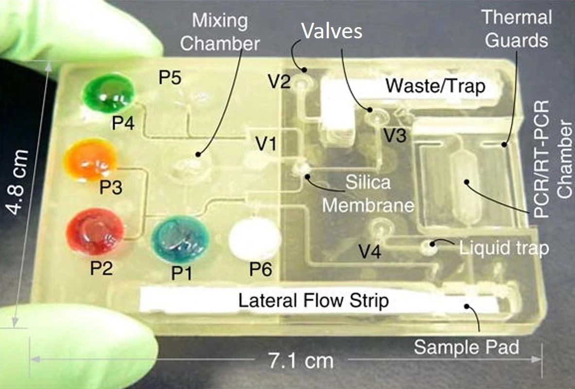
PC is a durable material created by polymerizing bisphenol A and phosgene, resulting in repeating carbonate groups. PC chips are often used in biomedical studies and bioanalyses, including sample lysis, nucleic acid isolation, amplicon labeling, and pathogen detection (Figure 10). This material is suited for DNA thermal cycling applications due to its transparency in the visible and its very high glass transition temperature (∼145 °C) [13].
However, PC has low stability against organic solvents, high background fluorescence, which is problematic when imaging fluorescently labeled biomolecules, and poor UV transmissivity, preventing UV polymerization inside PC channels. Notably, its optical properties can be optimized using different additives, chemical, or plasma treatment [3].
PC chips can be fabricated using our thermoplastic molding setup.
Cyclic olefin (co)polymer (COC/COP)
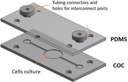
COC and COP are other popular biocompatible thermoplastic polymers used in microfluidic chip fabrication (Figure 11). In COC, chain copolymerization of cyclic monomers with ethylene is performed. The COP polymer is formed through ring-opening metathesis polymerization of cyclic monomers and subsequent hydrogenation.
Depending on the ethylene to cyclic monomer content ratio, COC has different grade variations that offer different mechanical and heat resistance properties. For instance, depending on their grade, COC/COP can provide better mechanical strength or heat resistance than PMMA and PC.
Furthermore, the transparency of COC/COP near UV is higher than PMMA and PC, which is advantageous for optical imaging and UV irradiation techniques to polymerize hydrogels and graft inside COC/COP microfluidics channels [18]. COC/COP also has high chemical resistance against acid and alkali corrosion, hydrolyses, and several organic polar solvents, such as methanol and acetone.
COC chips can be fabricated using our thermoplastic molding setup.
Thermoplastics are well suited for large-scale production; however, their accessibility and transferability to smaller scales remain problematic. This encourages the persistence of PDMS in this domain despite its flaws [1]. This also opened the way for paper to become a popular material for microfluidic chip fabrication.
Paper
Paper-based microfluidic chip started gaining significant popularity around 2007. Paper is a highly porous material with the ability to wick fluids. It is possible to create hydrophilic channels on paper, making the rest of the regions hydrophobic, where the fluid will be precisely guided through the hydrophilic region by the capillary effect. Paper is a promising material offering portable and low-cost analysis in bioassay-based personalized medical care.
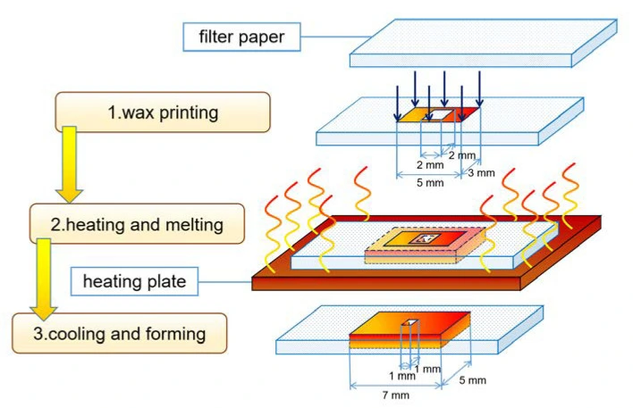
Paper-based chips can be fabricated using lithography or printing techniques. In the first one, a polymer solution is applied to the paper, and the formed coating is removed from the channel regions; this method is of high resolution but expensive. In contrast, printing methods require simpler equipment and directly generate hydrophobic barriers without exposing the channel area to reagents [2] (Figure 12).
There are several advantages of paper-based microfluidic chips:
1) there is no need for an external power source, as microchannels act as a passive pump dispenser
2) channels have a great surface-to-volume ratio and can be used to store reagents by simply drying the soaked area
3) paper is one of the cheapest materials, and the fabrication method is simple and low-cost
4) paper can filter out particles from the sample [2].
Along with these advantages come some challenges:
1) the detection sensitivity is low due to the channel’s fabrics, which can block the internal signal and dilute the sample
2) the fluid with lower surface tension, confined by the hydrophobic region, may not be properly guided through the channels
3) high-density fluids are complex to integrate as the minimal reported channel width is 200 µm, whereas 20 µm channel resolution is common for other materials
4) the problem of evaporation in open channels is also common in paper microfluidics [2].
Due to the limitations of traditional (PDMS, silicon, and glass) and recent materials (thermoplastics and paper), researchers started using composite materials for microfluidic chip fabrication.
Composite materials
Hybrid microfluidics devices were developed to take advantage of each material’s features while avoiding their limitations. Miniaturized paper/polymer hybrid microfluidics microplates (PMMA, PDMS, etc.) are cost-effective. They enable rapid immobilization of biomolecules and offer high performance in flow control, a feature that purely paper-based microfluidic chips can’t operate [21].
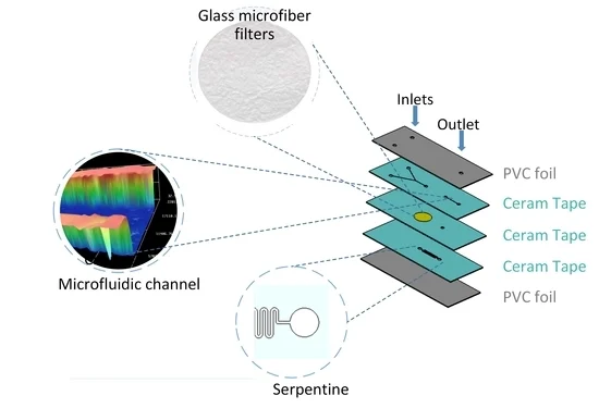
Koijc et al. proposed a composite, cost-effective chip that included polyvinyl chloride (PVC) soft foils between hard chips made of ceramic tapes in sandwich-like structures to form diaphragm valves (Figure 13). It presented good optical, mechanical, and thermal characteristics and excellent resistance to high flow rates. Moreover, each layer could be created and tested separately before lamination, achieving high reliability and reproducibility [22].
Gao et al. combined gas-permeable PDMS with a photocurable gas-impermeable polymer to enable the local control of oxygen tension in microfluidics cell cultures. Hypoxic zones of precise dimensions and geometry were established inside microfluidics cell culture chambers [23].
Deadlines of European Programmes 2026/2027
Get the MIC Horizon Europe 2026/2027 Calls Calendar:
-All Horizon Europe deadlines (by cluster and call).

Microfluidic chip fabrication approaches
The fabrication techniques required to process a given material have significant implications for the feasibility and transferability of the processes throughout diverse settings, such as small-scale lab production or large-scale industrial production.
Molding
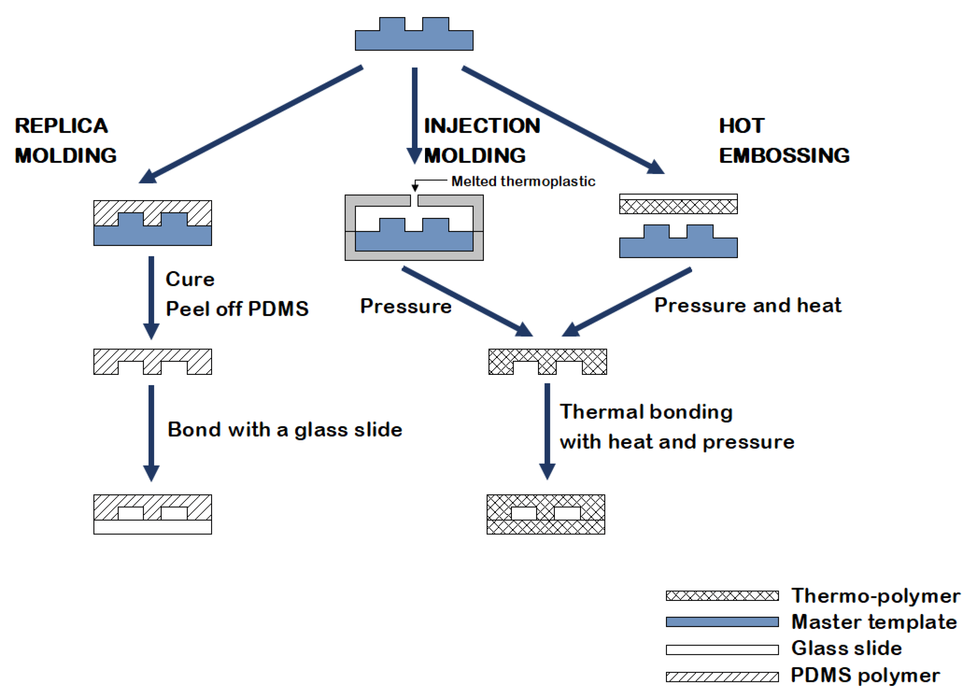
The main molding methods used for microfluidic chip fabrication are soft lithography, injection molding, and hot embossing (Figure 15).
Soft lithography
Soft lithography is one of the most popular methods for fabricating microfluidic chips. The technology uses photolithography to generate silicon and photoresist molds over which a liquid-set polymer such as PDMS is poured and cured. The cured polymer is peeled from the mold surface and contains a replica of the mold. A closed channel is formed by bonding the mold with a glass slide (Figure 15).
This method provides high-resolution replicas, generates intricate 3D flows, and produces high flexibility and optical transmittance designs. However, as the used materials are soft, pattern deformation may occur, especially when removing the cast from the mold. Moreover, high-resolution soft lithography requires a semi-cleanroom; nonetheless, rapid prototyping techniques brought high-resolution, low-cost methods that do not require a cleanroom [25, 26].
Injection molding
Injection molding and hot embossing utilize the range of available thermoplastics to generate high-throughput, cost-efficient, and precise microfluidics. Injection molding starts with transferring pre-polymerized thermoplastic pellets from a hopper into a heated barrel.
Accurate temperature control is critical to ensure the polymer melts uniformly without degradation. After the thermoplastic melts, it is injected under high pressure inside a heated mold cavity. The mold cavity is designed to replicate the microfluidic chip’s complex patterns, including channels, wells, and ports. The pressure is held for a specific period while the temperature is decreased below the polymer glass transition temperature. Once solidified, the material is ejected from the mold (Figure 15). This technique is advantageous in terms of costs and method simplicity. However, it is restricted to thermoplastics and has limited resolution [25, 26].
Hot embossing
Similar to injection molding, hot embossing involves melting thermoplastics and shaping them into molds using pressure and heat. First, a thermoplastic film is placed between two mold inserts. Next, the mold chamber is evacuated, compressed, and heated, creating a cast of the mold. Finally, the mold is cooled, and the cast is removed. Hot embossing has several advantages over injection molding (Figure 15).
Compared to injection molding, hot embossing requires the thermoplastic to flow a relatively small distance, significantly reducing the material’s stress. The cast’s shrinkage is also reduced, making this method effective in fabricating delicate designs. However, this technique is limited to thermoplastics and is difficult to employ in manufacturing complex 3D structures [25, 26].
3D printing
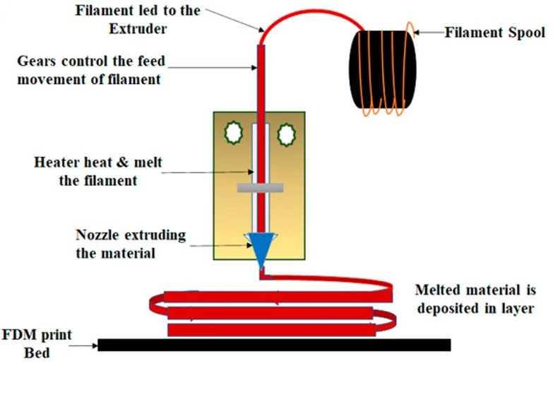
3D printing is a layer-by-layer manufacturing technology that adds a new material layer to the previous one and prints a 3D digital model. 3D printing technologies have great potential for microfluidics researchers and can be easily used for prototyping. Different technologies are associated with 3D printing, mainly fused deposition modeling (FDM), stereolithography (SL), and multijet modeling (MJM). These three methods require creating a 3D computer-aided design of the desired microfluidic chip, which is then converted to the stereolithography file that the printer uses to print the device [26].
Fused deposition molding
In fused deposition molding (FDM), the material is heated at a high temperature and extruded through a thin nozzle onto the stage in a predefined pattern. After the deposition of one layer, the stage moves down, and the next layer is deposited on top of the previous one (Figure 16).
Although FDM is cheaper, more user-friendly, and commercially successful than the other 3D printing techniques, it has some drawbacks, including the materials’ poor feature resolution and low optical transparency [4]. Moreover, compared to their injection-molded counterparts, FDM-printed blocks are more prone to compressive stress fracture, leak-prone, and filament sizes are relatively large for making microfluidics channels. Furthermore, FDM printing generates hazardous plastic fumes that would require ventilation [27].
Stereolithography
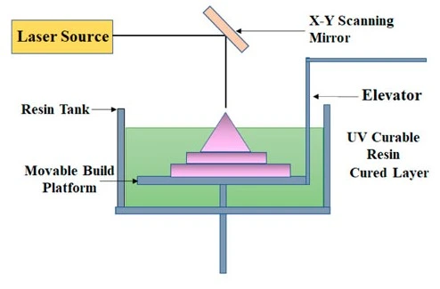
The stereolithography (SLA) method uses a laser or light-emitting diode (LED) to polymerize layers in a liquid photopolymer resin. Once the first layer is hardened, the stage moves vertically so that liquid resin covers the solid layer, which allows the next layer to be polymerized. This process is repeated until the microfluidic chip is complete [4] (Figure 17).
It operates particularly well for designing complex prototypes and small-batch productions. Significant advancements have been made in SLA, which now offers greater accuracy, quicker print times, and a wider variety of materials. For SLA to become usable in microfluidics, the resins must be biocompatible, such as hydrogel-based resins, including polyethylene-glycol-diacrylate (PEG-DA) [29].
Notably, greater functionality of SLA 3D printed devices has been demonstrated by Folch’s group, who generated implanted membranes using a higher molecular weight PEG-DA resin as a porous membrane [30]. Though SLA can achieve high resolutions, using multiple materials is difficult compared to MJM and FDM.
Multijet modeling
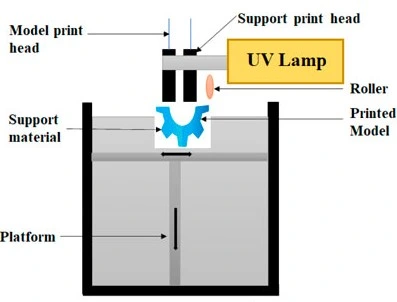
The multijet modeling (MJM) utilizes a photosensitive resin similar to SLA. It builds objects by jetting thousands of photopolymer droplets onto a built-in substrate and solidifying them with a UV light source. The printer consists of many printing heads and movable platforms. Each printing head is filled with many liquid resin types, and various materials can be sprayed and cured simultaneously (Figure 18).
This technique can fabricate complex accurate multi-material objects with smooth surface texture and high-resolution 3D objects of different modular strengths. However, MJM machines tend to be expensive, have difficulty producing features in the submillimeter range, and most resins are proprietary [26, 28].
Microfluidic chip bonding approaches
PDMS bonding
Silicon or glass can easily bond to PDMS through surface activation via oxygen plasma treatment or corona discharge method.
Surface activation aims to generate reactive chemical groups for covalent bonding. The terminal methyl groups (–CH3) in PDMS can be replaced by silanol groups (–Si–OH), and covalent siloxane bonds (Si-O-Si) can be formed (Figure 19). The processes taking place upon plasma/corona exposure can be quite complex since the material is simultaneously subjected to a mixture of energetic particles and radiation, which can cause at least 12 different interactions. The surface oxidation of PDMS and the increased concentration of hydroxyl groups can also form strong intermolecular bonds [31].

Oxygen plasma treatment
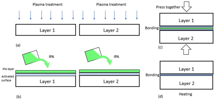
Plasma treatment is the most used method for PDMS surface activation. It involves exposing the material to ionized gas (plasma), making the surface more hydrophilic. Various gases can be used from medium vacuum to atmospheric pressure, depending on the purpose (e.g., oxygen, argon, nitrogen, hydrogen, etc.). For instance, low-middle vacuum range pressures are used to create a silanol-rich surface.
The surface activation process takes place inside a vacuum chamber. After plasma treatment, the layers are quickly aligned. Solvents can be applied to prevent further hydrophobic recovery, ensuring a strong, long-lasting bond between the layers (Figure 20).
For successful bonding, gas content, pressure, plasma power, and exposure time must be optimized; for example, using a common plasma chamber yields reproducible results and better bond quality. Low-pressure plasma is also less harmful to functional elements that might be integrated onto the treated surface than corona treatment [31].
Corona discharge
A corona treater is a device that generates a high voltage across an electrode. The high potential of the electrode ionizes the surrounding air, creating a localized plasma called corona discharge. The sample-electrode distance, movement speed, and treatment time must be precisely controlled. Corona treatment is a simple, cheap, portable, easy, and fast method that can be generated at room temperature and atmospheric pressure without the need for a vacuum system. However, the technique is usually performed manually, which can be a major drawback [31].
Thermoplastics bonding
Using oxygen or corona treatment to bond thermoplastics usually leads to weak bonding. The most common techniques to irreversibly bond thermoplastic polymers include thermal fusion, solvent, and chemical bonding. Factors such as transparency, resolution, precision of the microchannels, and bonding strength should be considered when choosing a suitable process [34].
Thermal fusion bonding
In thermal fusion bonding, the polymeric layers are heated above their glass transition temperatures (Tg), while the layers are pressed together using a hydraulic press or vacuum thermocompressor (Figure 21). The print, cut, and laminate (PCL) approach is used to fabricate polyester thermoplastics. COC and PMMA microfluidic chips are widely fabricated using the thermal fusion bonding method. Their exposure to UV light beforehand can reduce the bonding temperature to below the Tg as a short-wavelength UV light can break surface polymer chains.
Another alternative is to treat with oxygen plasma beforehand [34]. Thermal fusion bonding is a very fast technique. However, it requires high pressure and temperature, which can cause channel deformation and hinder its potential for the low-cost mass production of microfluidics devices [34].

Solvent bonding
In solvent bonding, an applied solvent diffuses across the polymer interface, dissolves, and compresses the polymer chains; then, as it evaporates, the induced mobile chains are entangled in each other and create a strong bonding force (Figure 22). The process is carried out at very low concentrations to avoid polymer deformation by the solvent, which increases the required bonding time. Solvent bonding is usually stronger when it is used for bonding layers with the same material and when it is integrated with thermal bonding [36].
Non-polar organic solvents, such as hydrocarbons, dissolve COC substrates. PC-PC bonding is done using an acetone and n-pentane mixture, and PMMA-PMMA bonding by a UV and solvent-assisted method. Solvent bonding is a longer process than thermal fusion, but it does not require high temperatures, which reduces the fabrication cost. However, overexposure to the solvent can result in microfluidics channel deformation, and solvent residue can adversely affect the functionality of immobilized biomolecules [31].

Chemical bonding
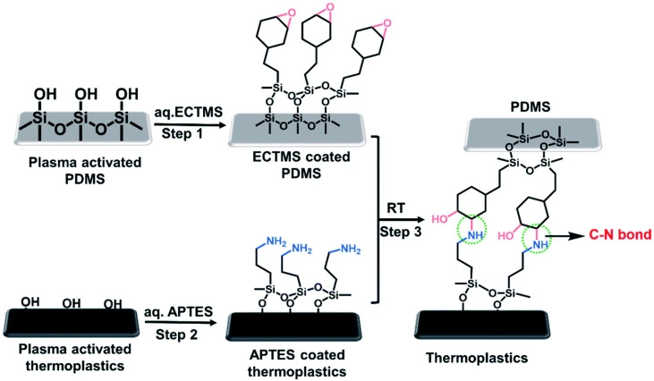
Chemical bonding uses functional groups to induce covalent reactions between polymeric layers at the interface. First, the surface of PDMS and thermoplastic substrates is activated via plasma treatment. Then, using silane reagents, thermoplastic is bonded to PDMS microchannels with strong covalent carbon-nitrogen bonds (Figure 23). This step is followed by oxygen plasma treatment after proper heat treatment [37].
Compared to thermal fusion and solvent bonding, chemical bonding allows the simultaneous functionalization of microchannels’ inner surface as the reactive groups can be incorporated for further covalent biomolecule attachment. In addition, this method results in superior bonding strength and allows bonding at low temperatures and pressures, which better preserves the precision of the channels’ geometry. However, chemical treatment of the layers involves many steps, making it troublesome for commercialization [31].
Conclusion - Pushing boundaries of microfluidics device fabrication
The vast array of materials available today and the numerous fabrication techniques provide many pathways for producing microfluidics devices. Each material and method offer distinct advantages, allowing for customization based on the specific requirements of a given application, whether biological testing, chemical analysis, or drug delivery. The rapid advancements in chip fabrication technologies further enhance precision, scalability, and cost-effectiveness, expanding the possibilities for innovation in microfluidics. However, researchers and industries must carefully balance these factors with the limitations of each material and technique. This trade-off requires strategic decision-making to ensure that microfluidic chips meet the specifications needed for their intended applications. Nonetheless, the continuous development of new materials and methods promises to push the boundaries of microfluidics device fabrication.
Funding and Support
This review was written under funding from the European Union’s Horizon research and innovation program HORIZON-CL4-2021-DIGITAL-EMERGING-01-27, grant agreement no. 101070120 (BIOPROS),
the European Union’s Horizon research and innovation program Marie Skłodowska-Curie grant agreement no. 956387 (LasIonDef),
and the French Agence Nationale de la Recherche (ANR), project ID: ANR-21-CE15-0045 (TREATABLE).



This review was written by Diana Kafizova, R&D engineer, and Celeste Chidiac, PhD.
Published in October 2024.
Contact: Partnership[at]microfluidic.fr


References
- MCMILLAN, A.H., M. Roeffaers, and S. Lesher-Pérez, Thermoplastic elastomer microfluidic devices for biology and chemistry. 2021, University of Vienna.
- Ren, K., J. Zhou, and H. Wu, Materials for Microfluidic Chip Fabrication. Accounts of Chemical Research, 2013. 46(11): p. 2396-2406.
- Shakeri, A., et al., Bio-functionalization of microfluidic platforms made of thermoplastic materials: A review. Analytica Chimica Acta, 2022. 1209: p. 339283.
- Nielsen, J.B., et al., Microfluidics: innovations in materials and their fabrication and functionalization. Analytical chemistry, 2019. 92(1): p. 150-168.
- Zhang, J., et al., Ultrafast Nucleic Acid Detection Equipment with Silicon-Based Microfluidic Chip. Biosensors, 2023. 13(2): p. 234.
- Nge, P.N., C.I. Rogers, and A.T. Woolley, Advances in Microfluidic Materials, Functions, Integration, and Applications. Chemical Reviews, 2013. 113(4): p. 2550-2583.
- Martinez, A.W., S.T. Phillips, and G.M. Whitesides, Three-dimensional microfluidic devices fabricated in layered paper and tape. Proceedings of the National Academy of Sciences, 2008. 105(50): p. 19606-19611.
- Folch, A., Introduction to bioMEMS. 2016: CRC press.
- Lin, L. and C.K. Chung, PDMS Microfabrication and Design for Microfluidics and Sustainable Energy Application: Review. Micromachines (Basel), 2021. 12(11).
- Gokaltun, A., et al., Recent advances in nonbiofouling PDMS surface modification strategies applicable to microfluidic technology. Technology, 2017. 5(01): p. 1-12.
- Kotz, F., et al., Fused Deposition Modeling of Microfluidic Chips in Polymethylmethacrylate. Micromachines, 2020. 11(9): p. 873.
- Wang, Y., et al., Recent progresses in microfabricating perfluorinated polymers (Teflons) and the associated new applications in microfluidics. Microphysiological Systems, 2018. 2.
- Giri, K. and C.-W. Tsao, Recent advances in thermoplastic microfluidic bonding. Micromachines, 2022. 13(3): p. 486.
- Jafari, A., et al., Surface properties and cell-surface interaction of polystyrene-graft-poly(2-hydroxyethyl methacrylate). Progress in Organic Coatings, 2024. 189: p. 108278.
- Trinh, K.T.L., et al., Rapid Fabrication of Poly(methyl methacrylate) Devices for Lab-on-a-Chip Applications Using Acetic Acid and UV Treatment. ACS Omega, 2020. 5(28): p. 17396-17404.
- Oliveira, M.J., et al., A simple polystyrene microfluidic device for sensitive and accurate SERS-based detection of infection by malaria parasites. Analyst, 2023. 148(17): p. 4053-4063.
- Chen, D., et al., An integrated, self-contained microfluidic cassette for isolation, amplification, and detection of nucleic acids. Biomed Microdevices, 2010. 12(4): p. 705-19.
- O’Neil, C.E., et al., Characterization of activated cyclic olefin copolymer: effects of ethylene/norbornene content on the physiochemical properties. Analyst, 2016. 141(24): p. 6521-6532.
- Kulsharova, G., et al., Development of a Hybrid Polymer-Based Microfluidic Platform for Culturing Hepatocytes towards Liver-on-a-Chip Applications. Polymers, 2021. 13: p. 3215.
- Jin, Y., et al., The Road to Unconventional Detections: Paper-Based Microfluidic Chips. Micromachines (Basel), 2022. 13(11).
- Zhou, W., et al., Recent innovations in cost-effective polymer and paper hybrid microfluidic devices. Lab Chip, 2021. 21(14): p. 2658-2683.
- Kojic, S.P., G.M. Stojanovic, and V. Radonic, Novel cost-effective microfluidic chip based on hybrid fabrication and its comprehensive characterization. Sensors, 2019. 19(7): p. 1719.
- Gao, Y., G. Stybayeva, and A. Revzin, Fabrication of composite microfluidic devices for local control of oxygen tension in cell cultures. Lab on a Chip, 2019. 19(2): p. 306-315.
- Ballacchino, G., et al., Manufacturing of 3D-Printed Microfluidic Devices for the Synthesis of Drug-Loaded Liposomal Formulations. International Journal of Molecular Sciences, 2021. 22(15): p. 8064.
- Niculescu, A.G., et al., Fabrication and Applications of Microfluidic Devices: A Review. Int J Mol Sci, 2021. 22(4).
- Gale, B.K., et al., A Review of Current Methods in Microfluidic Device Fabrication and Future Commercialization Prospects. Inventions, 2018. 3(3): p. 60.
- Au, A.K., et al., 3D‐printed microfluidics. Angewandte Chemie International Edition, 2016. 55(12): p. 3862-3881.
- Prabhakar, P., et al., 3D-Printed Microfluidics and Potential Biomedical Applications. Frontiers in Nanotechnology, 2021. 3.
- Iftekar, S.F., et al., Advancements and Limitations in 3D Printing Materials and Technologies: A Critical Review. Polymers, 2023. 15(11): p. 2519.
- Kim, Y.T., et al., Digital manufacturing of selective porous barriers in microchannels using multi-material stereolithography. Micromachines, 2018. 9(3): p. 125.
- Borók, A., K. Laboda, and A. Bonyár, PDMS Bonding Technologies for Microfluidic Applications: A Review. Biosensors (Basel), 2021. 11(8).
- Neves, L.B., et al., A Review of Methods to Modify the PDMS Surface Wettability and Their Applications. Micromachines (Basel), 2024. 15(6).
- Tony, A., et al., A Preliminary Experimental Study of Polydimethylsiloxane (PDMS)-To-PDMS Bonding Using Oxygen Plasma Treatment Incorporating Isopropyl Alcohol. Polymers (Basel), 2023. 15(4).
- Shakeri, A., et al., The Fabrication and Bonding of Thermoplastic Microfluidics: A Review. Materials, 2022. 15(18): p. 6478.
- Trinh, K.T.L., D.A. Thai, and N.Y. Lee, Bonding Strategies for Thermoplastics Applicable for Bioanalysis and Diagnostics. Micromachines, 2022. 13(9): p. 1503.
- Su, S., et al., One-step bonding and hydrophobic surface modification method for rapid fabrication of polycarbonate-based droplet microfluidic chips. Sensors and Actuators B: Chemical, 2019. 282: p. 60-68.
- Pečar, B., M. Možek, and D. Vrtačnik, Thermoplastic-PDMS polymer covalent bonding for microfluidic applications. Informacije Midem, 2017. 47(3): p. 147-154.
Check the other Reviews
FAQ - Choosing the optimal materials and fabrication techniques for microfluidic chip and tubing
Choosing between PDMS, glass, COC, COP, PMMA, and silicon substrates?
Not every material dominates across applications. Though PDMS handles rapid iterations well – thanks to elasticity around 1-3 MPa and features as fine as 10 micrometers via soft lithography – it suffers from absorbing non-polar compounds while allowing gases through. On the contrary, glass resists chemical reactions, transmits light efficiently, shows negligible absorption, withstands elevated heat, and seals irreversibly following plasma or voltage-driven bonding. Meanwhile, COC and COP stand out for their minimal background glow, clear imaging properties, and stronger defenses against organic solutes compared to silicone rubber, making them suitable for throwaway fluidic units and mass production via molded shaping. Though PMMA resists many fabrication methods well, it scratches easily; exposure to some solvents may also cause cracks due to internal stress. Fabrication using silicon allows extreme accuracy at the wafer scale – features like deep reactive ion etching enable channels below ten micrometers – with strong performance under high temperatures and aggressive chemicals, yet light cannot pass through.
The relative importance of gas permeability and small-molecule absorption, how is a big deal?
It is important when you are concerned with the stability of concentration or oxygen levels. PDMS can achieve over 400-600 Barrer with O2 to achieve a rapid exchange of gases (good at cell culture oxygenation, poor at volatile reagents). It is also hydrophobic so that it can adsorb hydrophobes (steroids, dyes), but changes on-chip concentrations by tens of percent in hours with no surface treatments or barrier coats. COC/COP and glass are very effective at non-absorbing most small hydrophobes, and they have orders of magnitude lower gas permeability.
How do I choose the right bonding technique while also understanding how it might fail?
Faster than conventional methods, oxygen-plasma treatment creates strong chemical links between PDMS and glass – or two PDMS layers – in just moments. Weak bonds often stem from insufficient surface activation. Blisters sometimes appear when water gets caught during sealing.
Near the glass-transition point, thermal bonding of COC, COP, or PMMA requires gradual changes in temperature and force. Sudden changes may crush microchannels. Smooth tool surfaces help maintain shape. Particles reduce adhesion, so work under filtered-air conditions. Success often comes when environmental cleanliness matches precision in heating cycles.
Using solvents on PMMA or polycarbonate works quickly, but may cause surface cracks or expansion. Hold components steady during assembly to reduce shape changes.
Firm seals form when glass joins silicon through anodic bonding – almost as strong as the wafer itself. Be cautious if the glass contains high levels of alkali. Mismatched expansion during heating can also cause problems.
Aim for burst pressures three times your max operating level as a starting point. Glass or silicon layers, when properly fabricated, frequently withstand 2-5 bar. Pressure tolerance of one to two bars is common with PDMS-glass sealed by plasma, provided the surfaces are clean and even. Strength drops if contact isn’t uniform across the bond.
Tubing: what do I do when deciding between PTFE/FEP, PEEK, and silicone elastomers?
Instead of listing options, think about how substances react – PTFE and FEP handle solvents well while offering little grip inside, yet their rigidity limits sharp turns despite stable fluid displacement. For high-pressure tasks, such as those above 100 bar in separation methods, PEEK stands out for its strength and compatibility with living systems, especially useful when channels are narrow, say, between 50 and 250 micrometers wide. On the other hand, silicone bends easily, making it ideal for rotary pump setups where flexibility matters most; however, it lets gases pass through readily and might release additives if not made to health standards. Though flexible PVC tubing works well in many cases, it may degrade when exposed to powerful solvents. Where high solvent resistance matters, alternatives perform better. When measuring fluorescence, material choice affects results: FEP, PEEK, or COC yields lower background signals. Shorter light paths help reduce unwanted emission pickup. Precision often hides in these details.
What steps can be taken to reduce unused space and prevent escapes at joints?
Compression fittings with ferrules work well. Alternatively, choose compact ports made for tiny fluid systems. Smooth inner diameter changes matter – match chip, tube, and valve sizes so flow stays steady without trapped zones. When dealing with under one microliter total volume, standard Luer parts take up too much space – switch to small M5 or UNF connectors, or glue thin metal tubing instead. Aim to keep extra volume at each joint below 50 to 100 nanoliters; using narrow 1/32-inch outer-diameter lines with brief ferrule lengths makes this possible. Test every setup at double the working pressure for ten minutes straight – any slow movement now means leakage later.
When moving from a single model to mass production, which method handles growth most effectively?
Start quick tests with PDMS or layered laser-cut materials; shift to thermoplastics once the layout settles. For consistent results – details between 25 and 100 micrometers – try hot pressing with nickel forms or micro-molding with steel tools. Each part repeats well, yet crafting molds takes several weeks and requires a high initial investment. At scale, individual units drop to just a few euros apiece. When extreme accuracy matters, like on wafers, glass, or silicon, they still fit the task – accept their higher cost per item for unmatched stability under heat and harsh chemicals.
What affects autofluorescence, along with image clarity? I want clear optical results.
What something is made of affects its glow – additives do too, along with how rough the surface feels. Glass and certain plastics like COC or COP hardly ever shine when lit up; others, such as PMMA or PC, may emit light in blue-green ranges. Smoothness counts just as much as what’s inside – the aim should be under one micrometer for average roughness on viewing areas. Stress patterns caused by harsh heat or solvents during joining must be avoided. When working with confocal or TIRF methods, matching standard coverglass depth (~170 micrometers) helps maintain image quality. One straightforward option is to attach PDMS blocks directly to those thin glass pieces.
Sterilization and biocompatibility: what is safe and what degrades?
Heat sterilization is suitable for glass and many metal types; however, without proper support, most thermoplastic materials deform under these conditions. Radiation methods such as gamma or electron beams work well with COC/COP, though slight changes in material behavior may occur. Ethylene oxide is compatible with a wide range of components but requires extended venting afterward. PDMS tolerates repeated heat exposure but expands when exposed to organic solvents; removing extractables through baking reduces contamination risks. For cell-based applications, thin protective films – such as parylene C or silicon dioxide-type coatings – or attaching polyethylene glycol can limit unwanted uptake of chemicals and surface binding.
Is it possible for MIC to assist in choosing materials, developing bonding methods, or moving processes to larger scales?
True – we handle these tasks regularly. Our team builds complete systems, including tailored microchips, detectors, flow controls, and small-batch channel networks. Material selection and joining methods are tested rigorously, with pressure and durability results clearly measured. Finished models arrive prepared for experimental verification. Within Horizon Europe groups, such efforts become solid project segments and technology-readiness demonstrations. Stronger planning around technical execution, risks, and application potential often follows. Success rates for grant applications typically rise about twice the standard odds when we contribute.

