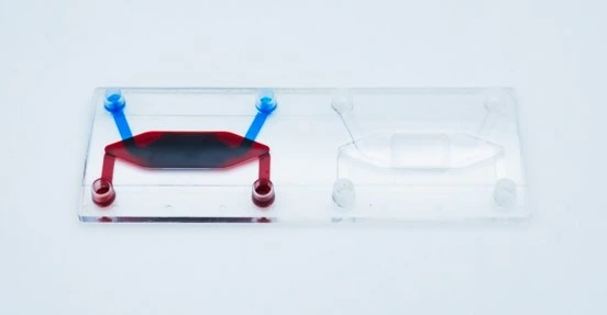
Thermoplastic Molding Microfluidics Setup
Move from PDMS to thermoplastic microfluidic chips
With only a few changes in your current microfabrication process
Compatible with different types of thermoplastic molding
COC, PMMA, PS, choose what best fits your needs
Fast process
Fabricate thermoplastic chips in only 1 hour
Need a microfluidic SME partner for your Horizon Europe project?
Thermoplastic molding microfluidics setup
Why switch to thermoplastic molding?
PDMS has been the working horse of microfluidics since its beginning. But as the technology matures, its limitations start to outweigh its perceived benefits, such as its easy and quick microfabrication process.
Researchers started looking for replacement materials, such as thermoplastics, because of limited chemical compatibility, high gas permeability, and low throughput.
However, thermoplastic molding for microfluidic chip fabrication can sound daunting, as it evokes extensive industrial facilities and complex machinery.

With that in mind, we challenged our capable team of engineers and researchers to come up with a way to adapt the current PDMS microfabrication process and turn it into a thermoplastic molding setup for microfluidic chip fabrication. And they were up to the challenge!
Let’s have a look at what they came up with:
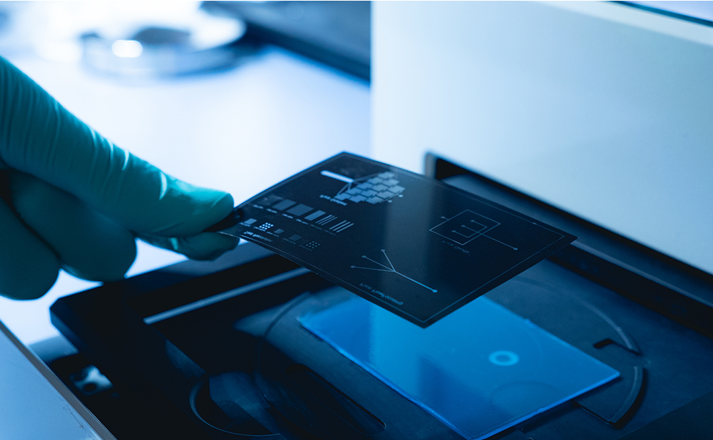
The PDMS microfabrication process starts with mixing PDMS with a curing agent and degassing inside a desiccator. Then, the elastomer is poured over the mold and cured in a conventional oven. Once ready, the chips are demolded and cut, and inlets are pierced with biopsy punchers. Lastly, the PDMS is bound to a glass slide after treatment in a plasma cleaner.
So, you only have to add our recommended heat press and laminator to your workflow and follow our instructions to be able to turn our PDMS microfabrication into a thermoplastic molding setup.
Your PDMS microfabrication process is different, and you don’t have all the listed equipment? Don’t worry; we’ve got you covered! We can provide you with all the necessary pieces and consumables; just drop us a line!
We recently published a review about the diverse materials and innovative fabrication and molding techniques used in microfluidic chip design.
Compatibility and applications
The thermoplastic molding setup can be used with:
PMMA device station
From mold development to high-resolution PMMA chip fabrication
✓ Fast process
✓ Multiple applications
✓ Simple and innovative setup
PMMA
COC polymer molding microfluidics setup
From PDMS to low-impurity high-performance COC polymer
✓ Fast process
✓ No need for a clean room
✓ Adaptable to your needs
COC
PS
Virtually any other thermoplastic
Applications are usually material-dependent, but in general terms, microfluidics chips produced with thermoplastic molding can be employed in:
Microfluidics nanomaterial synthesis pack
Microfluidics for production of nanomaterials using sheath flow focusing
✓ Efficient synthesis. ofnanomaterials
✓ Easy microfluidic system implementation
✓ Biomedical applications
Lab-on-a-chip applications (e.g. nanomaterial synthesis)
Gut-on-a-chip pack
Intestinal cells coculture under flow, mimicking the gut physiology
✓ All microfluidic pieces included, quick and easy assembly
✓ Dynamic culture conditions
✓ Advanced in viro/ex vivo
Gut-on-chip
Applications requiring specific-chip design and chemical inertia
Technical specifications
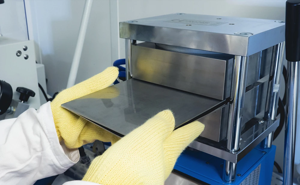
The thermoplastic molding microfluidic setup comprises:
Heat press with double heating plate
| Components | Technical specifications |
|---|---|
| Dimension | 420*550*680mm |
| Max temperature | 300℃ |
| Pressure range | 0-25 tons |
Laminator
| Components | Technical specifications |
|---|---|
| Dimension | 270*545*130 mm (L x w x h) |
| Max laminated width | 335 mm |
| Max laminated tickness | 35mm |
| Max temperature | 140 °C |
Options: Drilling machine
Consumables: Thermoplastic sheets of choice.
Frequently asked questions
Does the process also involve mold fabrication?
Currently, the thermoplastic molding microfluidic setup focuses on the chip fabrication and bonding from a pre-existing mold. However, we do have expertise to advise you in how to make your own molds.
What is the resolution of the thermoplastic microfluidic devices?
It depends on the chosen material, but for the PMMA devices done with this thermoplastic molding setup, for example, resolutions as low as 15 µm (channel width) for an aspect ratio of 2:1 can be achieved.
What maximum pressure can the devices withstand?
Based on internal testing, up to 3.5 bar.
What material can I use to close the chip?
The chip can be closed with a thermoplastic slide, a microscope glass slide or a microscopy-compatible polymer slide.
Is this process compatible with microscopy/reversed microscopy?
It depends on the properties of your thermoplastic of choice. PMMA, for example, is optically transparent and well-adapted to microscopy.

Funding and Support
The BIOPROS and MICRO4NANO projects results helped develop this instrument pack, with funding from the European Union’s Horizon research and innovation program under HORIZON-CL4-2021-DIGITAL-EMERGING-01-27, grant agreement no. 101070120 and the European Union under H2020-MSCA-RISE-2020, grant agreement No. 101007804.
Special thanks to Micaela Fernandes and Widad Mesbahi, who largely contributed to the development of this pack.
Products & Associated Accessories
FAQ - Thermoplastic Molding Microfluidic Setup
What problem does a “thermoplastic molding” workflow actually solve compared with classic PDMS chips?
PDMS is widely used in laboratories because it is flexible and can be prototyped quickly. However, when you require higher chemical compatibility, reduced gas permeability, higher reproducible throughput, or a route appearance more in line with actual manufacturing, PDMS can become restrictive. The thermoplastic molding system is simply a practical compromise: you retain the ethos of quick-and-dirty, but switch to thermoplastics (COC, PMMA, PS, and others) without turning your laboratory into a miniature microfabrication factory.
Will I have to discard my entire PDMS microfabrication workflow to switch to a different one?
Not really. The arrangement is such as to produce minimal disruption: you use hot-embossing instead of mixing, curing, and degassing in the early stages of PDMS, and you use drilling instead of inlet punching. Bonding still normally involves using the same plasma cleaner and an extra step of laminating chip closures. As a matter of fact, it is an upgrade to the workflow, not a complete reset.
What are the thermoplastics that it supports, and what is the selection procedure?
The pack is actually compatible with a number of typical thermoplastics (COC, PMMA, PS) and can be expanded to virtually any other thermoplastic, depending on your limitations. The logic behind a sensible choice is:
- PMMA is used when you want optical clarity and easy handling for microscopy-intensive work.
- COC at the expense of low-impurity, higher-performance polymer performance and expanded chemical strength.
- PS in cases where a familiar material is desired in many biology laboratories (and may also correspond well with cell culture requirements).
When you are not sure which the best material is, typically it is a best compromise in terms of solvent exposure, imaging requirements, mechanical, and downstream scale.
The real lab terms of how fast is the process?
The package is estimated at one hour manufacture cycle of a thermoplastic chip (assuming you have an already existing mold and you are on a fairly standard run). That is the main psychological change: thermoplastics cease to be slow and industrial, they become possible between meetings.
Is this installation with mold fabrication, or do I already have to have a mold?
The labor process is aimed at manufacturing and welding based on an already prepared model. MIC may also provide recommendations on the strategies of mold-making, should you have to invent your own molds (which can, in fact, be the actual bottleneck as you scale the prototype to repeatable production).
What solution can I possibly hope to get in channels and microfeatures?
Its solution is dependent on the thermoplastic and the processing conditions, although as a practical example: PMMA devices fabricated using this configuration have been reported with channel widths as small as 15 µm with the aspect ratio being approximately 2:1. Already, that is in a scale where much of the serious microfluidics (gradients, shear control, focusing structures) can be made possible without apology about the scale of features.
What do I to close the chip, and may I retain microscopy compatibility?
You can close the chip with:
- A thermoplastic slide
- A microscope glass slide
- Polymer slide of microscopic caliber
Microscope compatibility will depend on the thermoplastic you choose. An example of such a material is PMMA, which is optically transparent and can be used with standard and inverted microscopy. Given that imaging is your primary limitation, we advise you to make your choice of the closing substrate early, as it will inform most of your bonding and handling decisions.
What exactly is the hardware in the setup, and which specifications are most important to address?
The basic elements of the setup include:
- A heat press having two heating plates (max temperature 300 °C; range of pressures 0-25 tons; footprint approximately 420 x 550 x 680 mm).
- A laminator (max temperature 140 °C; maximum laminated width 335 mm; maximum laminated depth 35 mm; footprint approximately 270 x 545 x 130 mm).
Then you typically add:
- Drilling capability (for inlets/outlets) at will,
- Consumables: thermoplastic sheets of any material of your choice.
If you already have a plasma bonding capacity, this pack is intended as an addition, not a replacement.