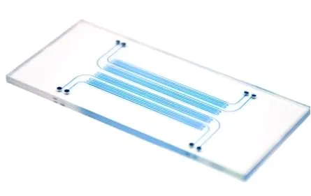
Polycarbonate (PC) Molding Microfluidics Setup
From PDMS to highly versatile and performant Polycarbonate PC
Fast process
Fabricate Polycarbonate chips in only 1 hour
No need for a clean room
Perform the whole microfabrication process outside of a clean room
High impact strength
Get chips that are resistant to high pressures and mechanical stresses
Need a microfluidic SME partner for your Horizon Europe project?
Polycarbonate modling microfluidics setup
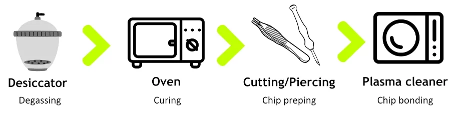
PDMS chip microfabrication
In our molding setup, the microfabrication of PDMS chips is performed outside of a clean room. Initially, PDMS is mixed with a curing agent and degassed in a desiccator. Then, the elastomer is poured onto a mold and cured in a conventional oven. Following curing, the chips are demolded, accurately cut, and inlet perforations are created using biopsy punchers. Lastly, the PDMS is firmly fixed to a glass slide following its treatment in a plasma cleaner.
However, due to PDMS limited chemical compatibility, high gas permeability, and low throughput, researchers started looking for replacement materials with better properties, such as thermoplastics.
Switching to Polycarbonate (PC) molding
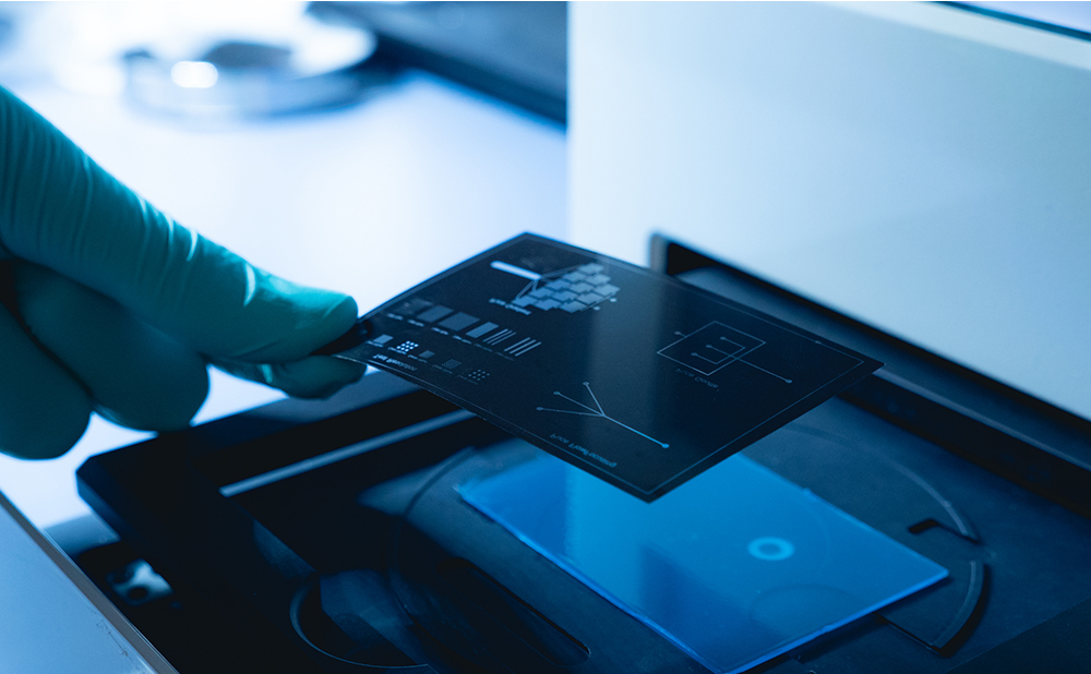
Polycarbonate (PC) is an optically transparent material, allowing for easy visualization and monitoring of fluids within microfluidic channels. In addition, it’s a durable and rigid thermoplastic material with high mechanical strength. Notably, this material is known for its excellent wide-range chemical resistance, biocompatibility, and commercial availability, which makes it adapted for mass manufacturing. Furthermore, PC is thermally stable, which confers resistance to elevated temperatures during fabrication processes and experimental operations on the fabricated microfluidic chips.
Overall, the combination of transparency, mechanical strength, chemical resistance, thermal stability, biocompatibility, and commercial availability makes polycarbonate a versatile and attractive material for fabricating microfluidic chips.
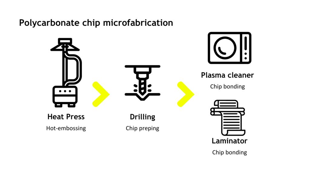
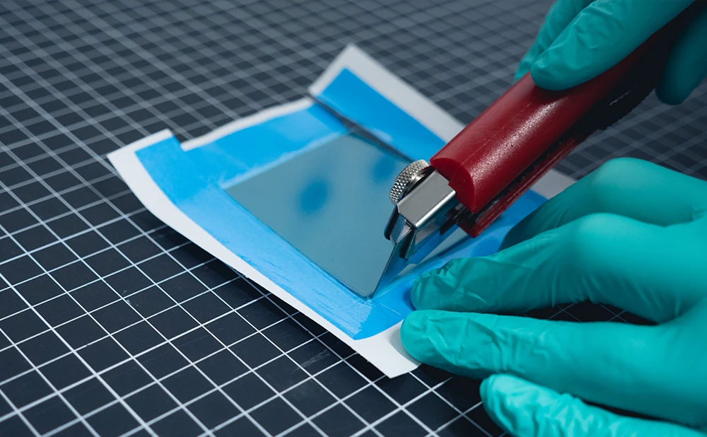
Polycarbonate microfabrication follows the same steps as thermoplastic chip microfabrication, and both can be performed outside of a clean room.
By integrating our recommended heat press and laminator into your workflow and adhering to our guidelines, you can seamlessly transition from PDMS microfabrication to PC material molding setup.
Your PDMS microfabrication process is different, and you don’t have all the listed equipment? Don’t worry; we’ve got you covered! We can provide you with all the necessary pieces and consumables; just drop us a line!
We recently published a review about the diverse materials and innovative fabrication and molding techniques used in microfluidic chip design.
Compatibility and Applications
The PC molding setup can also be used with:
PMMA device station
From mold development to high-resolution PMMA chip fabrication
✓ Fast process
✓ Multiple applications
✓ Simple and innovative setup
PMMA
Polystyrene (PS) molding microfluidics setup
From PDMS to highly versatile and transparent Polystyrene PS
✓ Fast process
✓ No need for a clean room
✓ High versatility
Polystyrene
COC polymer molding microfluidics setup
From PDMS to low-impurity high-performance COC polymer
✓ Fast process
✓ No need for a clean room
✓ Adaptable to your needs
COC
And many more!
Microfluidic chips produced with PC molding can be employed in:
Microfluidics nanomaterial synthesis pack
Microfluidics for production of nanomaterials using sheath flow focusing
✓ Efficient synthesis. ofnanomaterials
✓ Easy microfluidic system implementation
✓ Biomedical applications
Lab-on-a-chip applications (e.g. nanomaterial synthesis)
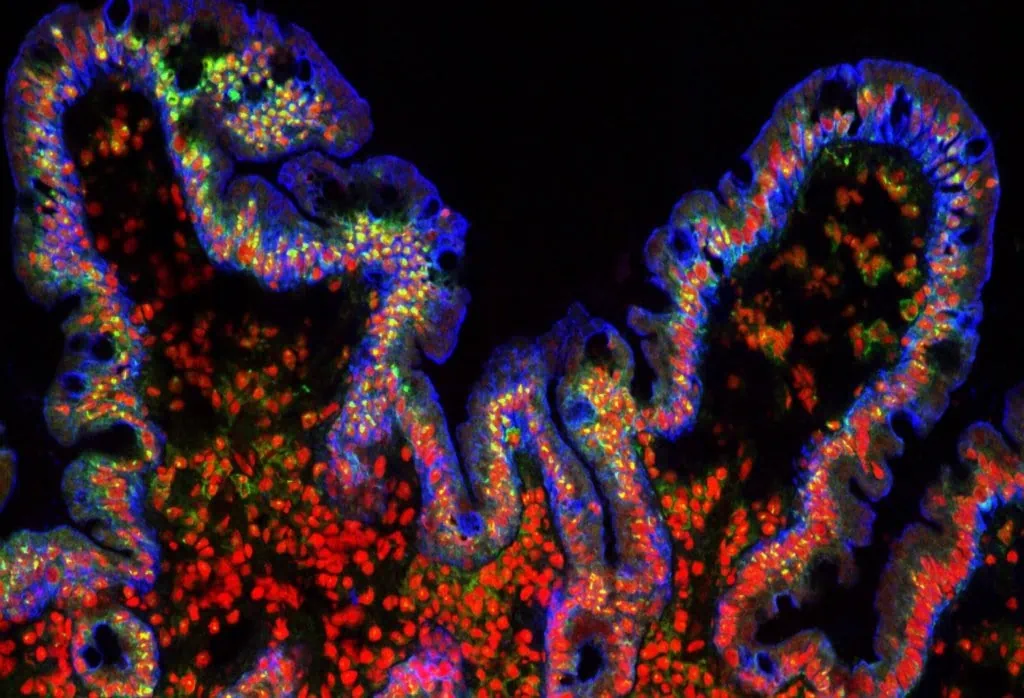
Gut-on-a-chip pack
Intestinal cells coculture under flow, mimicking the gut physiology
✓ All microfluidic pieces included, quick and easy assembly
✓ Dynamic culture conditions
✓ Advanced in viro/ex vivo
Gut-on-chip
Applications requiring specific-chip design and chemical inertia
And many more!
Technical specifications
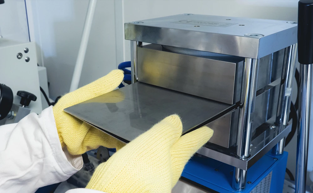
The polycarbonate (PC) molding microfluidic setup comprises:
Heat press with double heating plate
| Components | Specifications |
|---|---|
| Dimensions | 420*550*680mm |
| Max temperature | 300 °C |
| Pressure range | 0-25 tons |
Laminator
| Components | Specifications |
|---|---|
| Dimensions | 270*545*130 mm (L x w x h) |
| Max laminated width | 335 mm |
| Max laminated thickness | 35 mm |
| Max temperature | 140 °C |
Options: Drilling machine
Consumables: Polycarbonate sheets
Frequently asked questions
Does the process also involve mold fabrication?
Currently, the polycarbonate (PC) molding microfluidic setup focuses on the chip fabrication and bonding from a pre-existing mold. However, we do have expertise to advise you in how to make your own molds.
What is the resolution of the Polycarbonate microfluidic devices?
Resolutions as low as 15 µm (channel width) for an aspect ratio of 2:1 can be achieved.
What maximum pressure can the devices withstand?
Based on internal testing, up to 3.5 bar.
What material can I use to close the chip?
The chip can be closed with a thermoplastic slide, a microscope glass slide or a microscopy-compatible polymer slide.
Is this process compatible with microscopy/reversed microscopy?
Polycarbonate is optically transparent and well-adapted to microscopy.


Funding and Support
The BIOPROS and MICRO4NANO projects results helped develop this instrument pack, with funding from the European Union’s Horizon research and innovation program under HORIZON-CL4-2021-DIGITAL-EMERGING-01-27, grant agreement no. 101070120 and the European Union under H2020-MSCA-RISE-2020, grant agreement No. 101007804.
Products & Associated Accessories
FAQ - Polycarbonate (PC) Molding Microfluidics Setup
What is the actual problem, that the PC molding setup will fix, versus the “classic” PDMS chips?
PDMS is also convenient, but it has trade-offs: it is not compatible with many chemicals, has a high permeability to gases, and has a relatively low throughput. The PC molding solution is simply one that MIC considers a way to preserve the spirit of rapid iteration in microfluidics while moving to a more difficult-to-manufacture thermoplastic path. It is aimed at teams that desire machines that act more like actual engineering components (stiff, hard, consistent) and not squashy elastomers.
What is the time needed to manufacture a polycarbonate microfluidic chip using this system?
It takes approximately 1 hour to manufacture PC chips (including molding/embossing to finishing and sealing) assuming that you are starting with an existing mold and you have the major hardware already assembled.
Should I use a cleanroom to PC mold microfabrication?
No, that is one of the points of the headline. This is intended to be done in a place that is not in a clean room and this is significant to European labs who do not want to meter out each generation on shared cleanroom times (or consortia partners who require reproducible fabrication but do not want to have a heavy infrastructure).
What is the rudimentary logic of fabrication- what is different about PDMS?
PDMS normally implies: mix + degas, pour on mold, cure, demold, punch inlets, plasma bond to glass.
The transition to a thermoplastic manufacturing process is the focus of PC molding: the cumbersome stage of curing elastomer is substituted with hot embossing; the chips are prepared with drilling tools; and finally, a plasma cleaner and a laminator are used to close the seal. Practically, that is the way to achieve speed and more solid objects without transforming your laboratory into a microfabrication plant.
What is so good about polycarbonate as a microfluidic material (and when should it be a bad choice)?
PC is said to be optically transparent, mechanically robust and thermally stable with a broad chemical resistance and biocompatibility. The said properties are what make it frequently used when you are concerned with a higher pressure, mechanical life, or a more industrial handling. It is also commercially available, but it is unobtrusive in terms of scaling and repeatability.
In which case it is a bad idea: when you demand a highly solvent-selective profile of solvents, or an autofluorescence level close to zero, you will want to check this early against your optics/chemistry requirements (PC is great, but not magic).
What decision can I possibly achieve in the microchannels?
Channel widths to 15 um with aspect ratio of 2:1 (a low-end resolution standard) have been reported by MIC reports. It would be sufficient already to a lot of cell-handling, transport, gradients, and many lab-on-chip architectures- particularly when you are not aiming to make showpieces in the area of ultra-fine lithography.
What is the tolerance of the pressure of using these PC devices?
According to internal MIC testing, the devices can withstand a pressure of 3.5 bar. Granted, you run your experiments near that limit (or even make aggressive flow transients), then it is prudent to consider 3.5 bar as a known reference point, as opposed to a design point and to discuss margins, fittings, and sealing strategy with the team.
What are the practical contents of the equipment comprised by the “setup”?
What are the practical contents of the equipment comprised by the “setup”?
The basic hardware is simple and deliberately lab-friendly:
- Heat press with two heating plates: 420 x 550 x 680 mm, maximum temperature 300 °C, and pressure 0-25 tons.
- Laminator: size 270 x 545 x 130 mm, laminated maximum width 335 mm, laminated maximum thickness 35 mm, maximum temperature 140 °C.
- Optional: drilling machine
- Materials Fireproofing: polycarbonate sheets.
Is it provided in the process of fabrication of the mold, or do I have to provide my own mold?
The system concentrates on fabrication and bonding of chips out of an existing mold. With these words said, MIC also expressly states that they can recommend how to make your own molds- which is often the actual bottleneck in shifting teams away off PDMS (where molds are often made in-house through soft lithography) and thermoplastics (where the subject of mold strategy turns into a design and manufacturing choice).
What is the closing / sealing of the chip and whether it can be microscoped (inverted microscopy also?)
To close it down, MIC suggests that you can close PC chips with:
- a thermoplastic slide, or
- a microscope glass slide, or
- a polymer slide that is microscopy-compatible.
And yes, PC is optically transparent to the eye and “commonly suited to microscopy,” which encompasses the general requirements of inverted microscope operations (unless you select an incompatible bottom substrate and thickness to use as your objective working distance).
What are the alternative possibilities (when I am not certain PC is the correct choice)?
MIC also focuses on PC molding together with other thermoplastic applications such as PMMA device station, Polystyrene (PS) molding, and COC polymer molding. That can be useful in the real-world project context, in which you can select materials based on what is most important (optics, chemistry, mechanical robustness, biological use-case, supply chain), but still maintain something like a fast, no cleanroom mentality.