How to choose the best chip material for microfluidic fabrication?
Author
Celeste Chidiac, PhD
Publication Date
Keywords
PDMS
Thermoplastics
optical clarity
Composite
mechanical strength
gas permeability
Need advice for your chip materials?
Your microfluidic SME partner for Horizon Europe
We take care of microfluidic engineering, work on valorization and optimize the proposal with you
Introduction
The selection of chip material for microfluidic fabrication depends on various properties, including optical clarity, mechanical strength, gas permeability, and surface wettability. Conventional materials like glass and silicon were initially used due to their precision and stability, but they have cost and fabrication limitations. This led to exploring alternative materials, including elastomers, thermoplastics, paper, and composites, to enhance manufacturability and functionality in various applications.
Chip material | Advantages | Limitations | Applications |
Silicon | – High chemical and thermal stability | – Opaque, limiting optical applications | – MEMS integration |
Glass | – Optical transparency | – Complex and expensive fabrication | – Capillary electrophoresis (CE) |
PDMS | – Low cost | – High biomolecule adsorption | – Rapid prototyping |
Thermoplastics | – Low cost | – Some types have low chemical resistance | – Disposable microfluidic chips |
Paper-based microfluidic | – Low cost | – Low detection sensitivity | – Point-of-care diagnostics |
Silicon chip material
Silicon was one of the first microfluidic materials used due to its semiconducting properties, availability, ease of fabrication, chemical resistance, and thermal stability. However, its opacity limits its use in optical applications, and its fragility makes it unsuitable for incorporating active components like pumps and valves. Despite these drawbacks, silicon-based microfluidic chip materials are still employed in high-precision applications such as point-of-care diagnostics and organ-on-a-chip devices [1].
Glass chip material
Glass is a transparent and electrically insulating material with excellent chemical resistance, biocompatibility, and thermal stability. However, glass chip fabrication is complex and expensive, requiring high temperatures, pressures, and stringent environmental conditions for bonding. These challenges have limited its widespread, leading to the search for alternative materials [1]. One of its primary applications is capillary electrophoresis (CE).
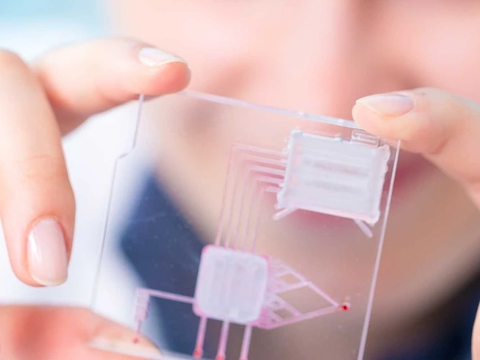
Elastomer chip material
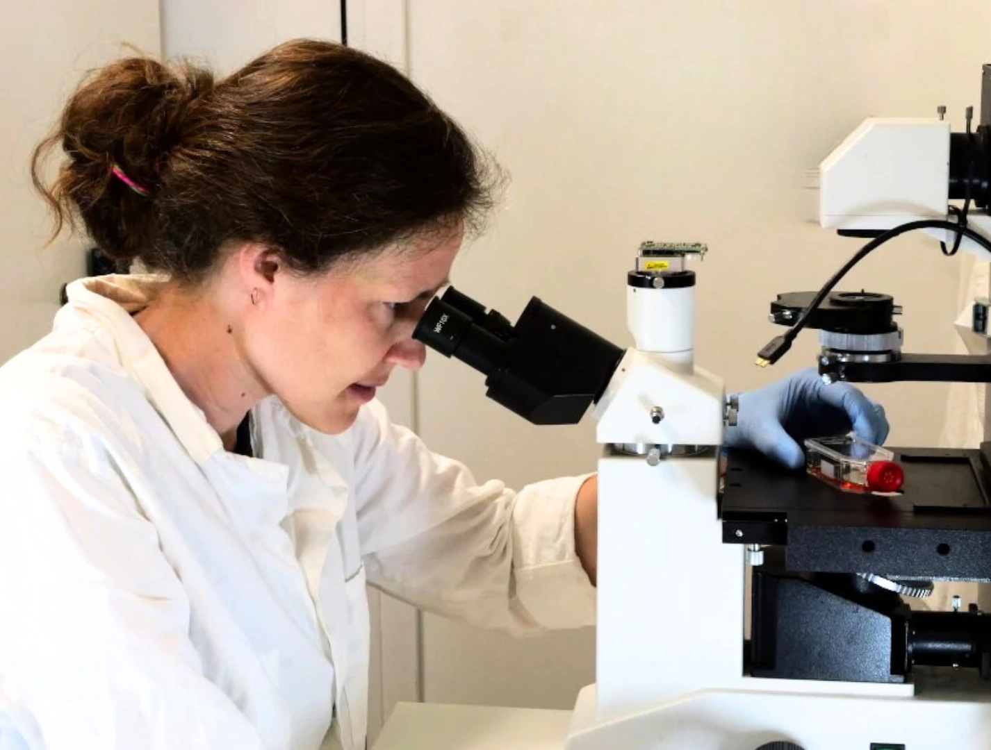
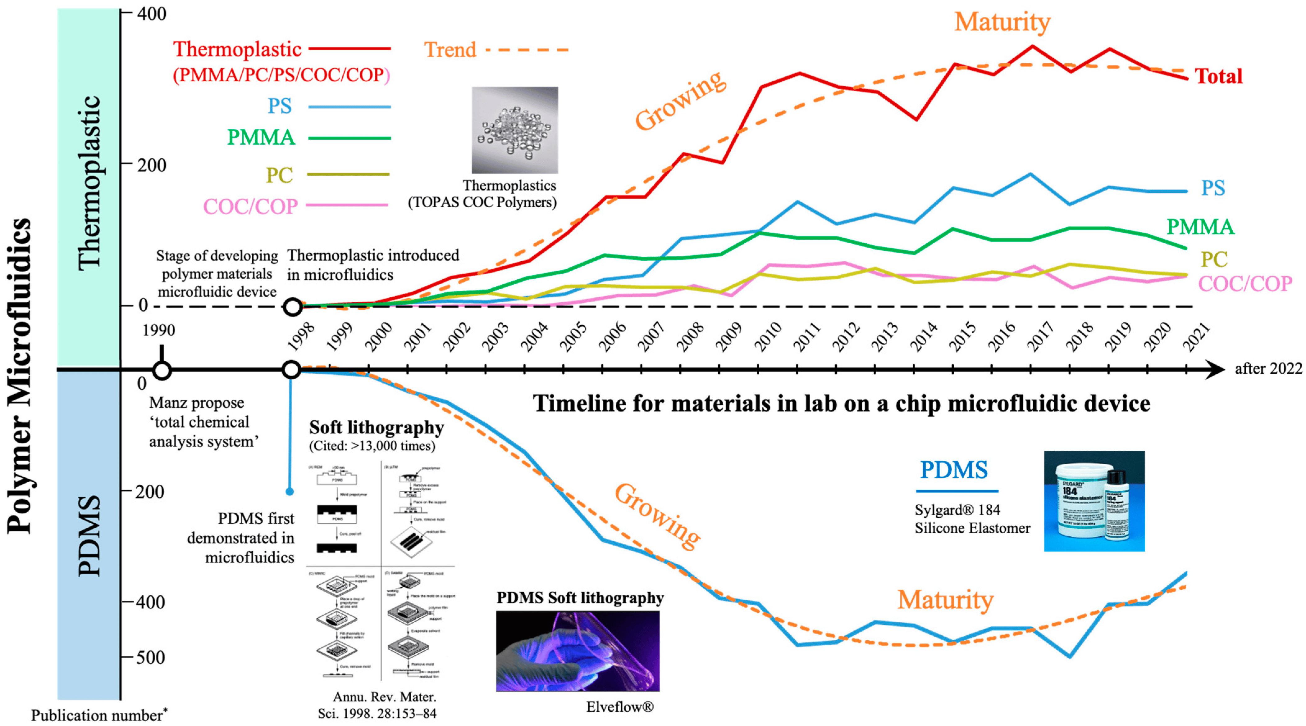
- Polydimethylsiloxane (PDMS): PDMS has revolutionized microfluidic since its introduction in 1998 due to its low cost, optical transparency, biocompatibility, and ease of molding [3]. It is particularly useful for rapid prototyping, as it allows for the quick fabrication of microfluidic devices through conventional machining or photolithography. However, PDMS has limitations, including poor surface treatment stability, high biomolecule adsorption, and chemical incompatibility with organic solvents, which restrict its use in biomedical applications [4]. Despite these drawbacks, it remains a popular choice in academic research and rapid prototyping.
- Perfluorinated polymers: Teflon-based materials provide an alternative to glass and silicon by offering high chemical inertness, non-stick properties, and optical transparency. These chip materials resist swelling, prevent biofouling, and are compatible with all solvents, making them attractive for advanced chemical and biological applications. However, their high cost and fabrication complexity limit their broad adoption [5].
Thermoplastic chip material
Thermoplastics became popular as microfluidic chip material in the early 2000s due to their low cost, rapid production, and scalability. They are crosslinked polymers that can retain their shape after cooling, making them suitable for micro-machining processes [2].
Various thermoplastics offer different advantages:
- Poly(methyl methacrylate) (PMMA): One of the most widely used thermoplastics, PMMA chip material is valued for its optical clarity, low price, and compatibility with electrophoresis applications. However, it has limited stability against organic solvents and poor UV transmissivity, which may restrict its use in specific applications [6].
- Polystyrene (PS): PS is commonly used in cell culture and biomedical assays due to its biocompatibility, optical transparency, and commercial availability. It is naturally hydrophobic but can be modified to improve cell adhesion and surface properties. Despite its advantages, expensive equipment is often needed for proper surface treatment [7].
- Polycarbonate (PC): PC is a stronger and more heat-resistant alternative to PMMA, offering excellent optical transparency and biocompatibility. It is frequently used in DNA thermal cycling and pathogen detection applications. However, its low stability against organic solvents and high background fluorescence are challenging for imaging techniques [6].
- Cyclic Olefin (co)polymers (COC/COP): These chip materials are known for high chemical resistance, superior optical properties, and compatibility with UV-based imaging techniques. COC/COP polymers have been used in hydrogel polymerization and grafting inside microfluidic channels, making them valuable for biomedical and analytical applications [8].
Paper chip material
Paper-based microfluidics gained significant popularity around 2007 due to its low-cost, ease of fabrication, portability, and capillary-driven flow transport without external power sources. However, challenges such as low detection sensitivity, difficulty guiding low-surface-tension fluids, and evaporation issues have limited its use. However, paper microfluidic remains a promising approach for point-of-care diagnostics and bioassay-based applications [9].
Composite materials
To overcome the limitations of individual materials, researchers have developed composite microfluidic devices that combine materials to optimize performance. For example, paper/polymer offers rapid immobilization of biomolecules and high performance in flow control. Another design uses polyvinyl chloride (PVC) layers and ceramic tapes to create microfluidic devices with high reliability, reproducibility, and flow control. These innovations offer a balance between cost, manufacturability, and functionality [10].
Want to know more on this subject? Check the extended review comparing the different chip materials and fabrication techniques.
Conclusion
Microfluidic chip fabrication has evolved from traditional chip materials like glass and silicon to more cost-effective and scalable alternatives such as polymers, thermoplastics, paper, and hybrid composites. While glass and silicon offer precision and chemical resistance, PDMS and thermoplastics have gained popularity due to their ease of manufacturing and biocompatibility. Paper-based microfluidic presents a promising low-cost alternative but faces challenges in fluid control and sensitivity. Meanwhile, composite materials offer a hybrid approach to overcoming individual material limitations. As research continues, developing new materials and fabrication techniques will further enhance the capabilities and accessibility of microfluidic technologies.
Funding and Support
This review was written under funding from the European Union’s Horizon research and innovation program HORIZON-CL4-2021-DIGITAL-EMERGING-01-27, grant agreement No. 101070120 (BIOPROS),
and the European Union’s Horizon research and innovation program Marie Skłodowska-Curie grant agreement No. 956387 (LasIonDef).

![]()
![]()

This review was written by Celeste Chidiac, PhD.
Published in February 2025.
Contact: Partnership[at]microfluidic.fr

References
- Nielsen, J.B., et al., Microfluidics: innovations in materials and their fabrication and functionalization. Analytical chemistry, 2019. 92(1): p. 150-168.
- Giri, K. and C.-W. Tsao, Recent advances in thermoplastic microfluidic bonding. Micromachines, 2022. 13(3): p. 486.
- Martinez, A.W., S.T. Phillips, and G.M. Whitesides, Three-dimensional microfluidic devices fabricated in layered paper and tape. Proceedings of the National Academy of Sciences, 2008. 105(50): p. 19606-19611.
- Gokaltun, A., et al., Recent advances in nonbiofouling PDMS surface modification strategies applicable to microfluidic technology. Technology, 2017. 5(01): p. 1-12.
- Wang, Y., et al., Recent progresses in microfabricating perfluorinated polymers (Teflons) and the associated new applications in microfluidics. Microphysiological Systems, 2018. 2.
- Shakeri, A., et al., Bio-functionalization of microfluidic platforms made of thermoplastic materials: A review. Analytica Chimica Acta, 2022. 1209: p. 339283.
- Jafari, A., et al., Surface properties and cell-surface interaction of polystyrene-graft-poly(2-hydroxyethyl methacrylate). Progress in Organic Coatings, 2024. 189: p. 108278.
- O’Neil, C.E., et al., Characterization of activated cyclic olefin copolymer: effects of ethylene/norbornene content on the physiochemical properties. Analyst, 2016. 141(24): p. 6521-6532.
- Ren, K., J. Zhou, and H. Wu, Materials for Microfluidic Chip Fabrication. Accounts of Chemical Research, 2013. 46(11): p. 2396-2406.
- Kojic, S.P., G.M. Stojanovic, and V. Radonic, Novel cost-effective microfluidic chip based on hybrid fabrication and its comprehensive characterization. Sensors, 2019. 19(7): p. 1719.
Check the other Reviews
FAQ - How to choose the best chip material for microfluidic fabrication?
How quickly can you narrow down a semiconductor material for your test?
Begin by acknowledging fixed factors like chemical environment – think solvents, pH, surfactants – as well as optical needs such as imaging type and light wavelength. Bonding strategy matters too, whether it allows reassembly or must be sealed permanently. Production scale shifts choices: a single device differs greatly from a batch of 10,000. As a guide, materials are split into roles. Glass or silicon is suited to aggressive chemicals or heat-intensive processes. When speed matters in early testing, PDMS stands out, especially with its flexible valve designs. For mass-produced, throwaway systems, thermoplastics – including PMMA, PS, PC, and COC/COP – are common picks. Paper-based or mixed-layer structures are best when cost is critical, and fluid flow relies solely on wicking.
Polydimethylsiloxane appears frequently across research settings. Could there be reasons beyond habit for its widespread adoption?
Speed comes cheap – soft lithography moves fast, channels stay transparent, yet bonding stays straightforward. Still, biology and chemistry face real hurdles: surfaces grab onto small hydrophobic molecules, proteins stick too well, treated layers wear off, and certain solvents cause problems. Useful for early designs and valve-based systems, though shaky when measuring responses involving greasy drugs or detergents without added protection or different base materials.
What if glass remains the best choice today?
For applications like capillary electrophoresis or high-NA fluorescence, where a material must resist chemicals, work safely in biological settings, insulate electrically, and remain optically clear, glass is a top choice. Although processing and joining parts require intense heat and pressure – making steps harder and costlier – it’s often selected because the experimental demands leave little room for alternatives. Some groups pick it simply because of its stable shape over time, even if speed isn’t on their side.
Yet silicon – dense yet accurate – where does it truly perform?
When it comes to fine detailing in tiny structures, silicon stands out due to its consistency under heat and compatibility with micro-electromechanical systems. In applications such as lab-on-a-chip devices or portable diagnostics, built-in sensing elements or heating components often compensate for poor light transmission through the material. Yet brittleness remains an issue, alongside challenges in embedding fluid control parts directly into the chip – factors that lead researchers toward alternatives such as glass or plastic unless electrical behavior is critical. Despite strengths in specific areas, practical limitations shape how widely it gets adopted.
Thermoplastics feel like the industrial middle ground. How do the main families differ?
What makes thermoplastics stand out is their role somewhere between rigid and flexible materials.
Poly(methyl methacrylate) is cheap, transparent, and commonly used in electrophoretic applications – yet it resists solvents poorly while allowing little ultraviolet light through.
It just works well with cells and stays clear. Not wet easily by water, though that can change if needed. Fixing the surface usually requires special tools.
When comparing materials, polycarbonate stands out due to its higher impact resistance and better performance under heat. Its optical clarity enables applications such as DNA amplification via temperature changes. Unlike acrylic, it withstands repeated heating without deforming. However, exposure to certain solvents may cause degradation over time. Imaging techniques can be affected by unwanted fluorescent signals from the material itself. Careful handling reduces risks during experimental use.
COC/COP stands out due to its sharp optical clarity. Despite minimal moisture absorption, it holds up well under ultraviolet light. Resistance to many chemicals makes it suitable for demanding applications. Often chosen for hydrogels formed by light-triggered polymerization. Found in devices for biological analysis because performance stays consistent. Its reliability supports precision without adding complexity.
In the 2000s, adoption grew fast – scaling capability made these methods stick. Hot embossing shifted easily into production, just like injection molding. Laser techniques followed a similar path, bridging research and manufacturing without fuss.
Now here’s a thought: paper-based microfluidics – how does it perform once past the prototype stage?
When tests run on capillary force without electricity – like basic medical checks – paper stands out because it costs little, moves easily, and shapes quickly. Yet poor signal detection, liquid loss during drying, and imprecise flow handling hold it back when exact measurements matter. Combining paper with polymer layers or adding wettable zones improves performance slightly, still avoiding high material expenses.
Fascinating materials, composites. How do hybrid chips benefit my work?
Putting different materials together – like paper with polymer or polymer with ceramic – lets their individual traits combine: one might resist wear well, another allows selective molecule passage, a third supports chemical bonding on its surface. Think of layered PVC paired with ceramic tape, built to manage fluid flow without failing easily. Or consider paper topped with a polymer, helping biological molecules stick quickly while directing liquid through tiny channels via capillary action. These combined structures frequently balance function and ease of production better than single-material options ever could.
What drives the decision when considering adhesion methods and coating adjustments?
A material’s processing limits depend on what it is made of and how its parts will react. High heat and pressure are ideal for glass, yet many materials cannot withstand such conditions. Plasma creates bonds in soft polymers like PDMS, though performance fades over time. Some plastics allow glue-free joining through heat, sound, or chemicals – methods suited to large-scale production. Surfaces that attract water may lose function unless protected. Lifespan matters when sensitivity affects results, so define storage duration or build in renewal steps.
What numbers should I keep in mind when pitching a Horizon Europe work plan?
One way to meet reviewer expectations is by linking technology readiness levels directly to materials and production scale. Prototypes at TRL 3-4 often rely on PDMS because it allows fast iteration. Moving into TRL 5-6 demands more durable options – thermoplastics fit here due to ease of molding and quality control. Where reactions involve extreme heat or chemical sensitivity, glass or silicon becomes necessary. Progress hinges not just on material but on how parts will be made – shifting from hot embossing to injection molding shows foresight. Testing must happen under realistic conditions, using representative samples. Experience suggests setting both material and bonding methods early – ideally by month six – to avoid delays down the line. Teams drafting EU submissions may find guidance in the MIC publication, which clearly outlines each phase transition.
What is the point of introducing a specialized SME, the Microfluidics Innovation Center (MIC), to your consortium?
Due to the interdependence of materials, bonding, and fabrication. MIC includes the design of intricate systems, microfabricated custom chips in glass/thermoplastics/PDMS, manufacturable bonding processes, and integration with scientific automation. Outside engineering, MIC also aids proposal writing and valorization; in most EU consortia, our participation normally increases proposal success rates twice the official rate by threefold prototyping and a sharp exploitation path.
What hidden challenges do scholars often overlook?
Start with the toughest chemicals when testing. Adsorption and leaching are clearly evident in PDMS, so watch closely. After treating surfaces, check instrument alignment – wettability shifts can skew results. Switching materials late, such as moving from PDMS to COC or glass, often disrupts timelines because solvents or imaging requirements change midway. Plan material choice at the outset. Bond strength and surface behavior need full attention from day one – they shape performance just as much as geometry or flow.