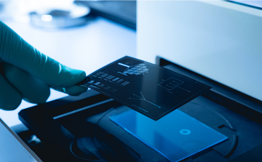
Polystyrene (PS) Molding Microfluidics Setup
From PDMS to highly versatile and transparent Polystyrene PS
Fast process
Fabricate Polycarbonate chips in only 1 hour
No need for a clean room
The whole microfabrication process is performed outside of a clean room
High versatility
Easily molded into various shapes and sizes
Need a microfluidic SME partner for your Horizon Europe project?
Polystyrene modling microfluidics setup
PDMS chip microfabrication
PDMS is the most commonly used material for the fabrication of microfluidic devices.
In our molding setup, the microfabrication of PDMS chips is performed outside of a clean room and begins by blending PDMS with a curing agent and degassing inside a desiccator. Then, the elastomer is carefully poured onto the mold and undergoes curing in a conventional oven. After completion, the chips undergo demolding and precise cutting, while inlet perforations are made using biopsy punchers. Finally, the PDMS is securely attached to a glass slide following treatment in a plasma cleaner.
However, PDMS limited chemical compatibility, high gas permeability, and low throughput are reasons why researchers started looking for replacement materials, such as thermoplastics.
Switching to Polycarbonate (PS) molding
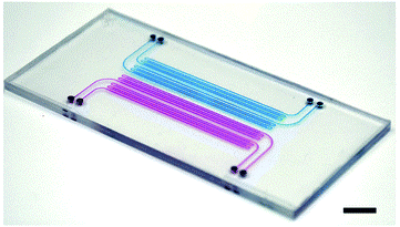
Polystyrene (PS) is a particularly interesting thermoplastic for chip microfabrication due to its many advantages. It’s an inert, rigid, biocompatible, and commercially available material adapted for mass manufacturing. Its low production costs present a cost-effective option for various applications. Moreover, transparent grades of PS are available, making it suitable for applications where visibility is important. Furthermore, PS material can be easily molded into various shapes and sizes, offering versatility in design and applications.
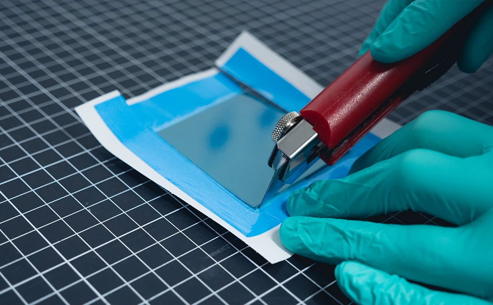
Polystyrene microfabrication follows the same steps as thermoplastic chip microfabrication, and both can be performed outside of a clean room.
By integrating our recommended heat press and laminator into your workflow and adhering to our guidelines, you can seamlessly transition from PDMS microfabrication to PS material molding setup.
Your PDMS microfabrication process is different, and you don’t have all the listed equipment? Don’t worry; we’ve got you covered! We can provide you with all the necessary pieces and consumables; just drop us a line!
We recently published a review about the diverse materials and innovative fabrication and molding techniques used in microfluidic chip design.
Compatibility and applications
The PS molding setup can also be used with:
PMMA device station
From mold development to high-resolution PMMA chip fabrication
✓ Fast process
✓ Multiple applications
✓ Simple and innovative setup
PMMA
Polycarbonate (PC) molding microfluidics setup
From PDMS to highly versatile and performant Polycarbonate PC
✓ Fast process
✓ No need for a clean room
✓ High impact strength
Polycarbonate
COC polymer molding microfluidics setup
From PDMS to low-impurity high-performance COC polymer
✓ Fast process
✓ No need for a clean room
✓ Adaptable to your needs
COC/COP
And many more!
Microfluidic chips produced with PS molding can be employed in:
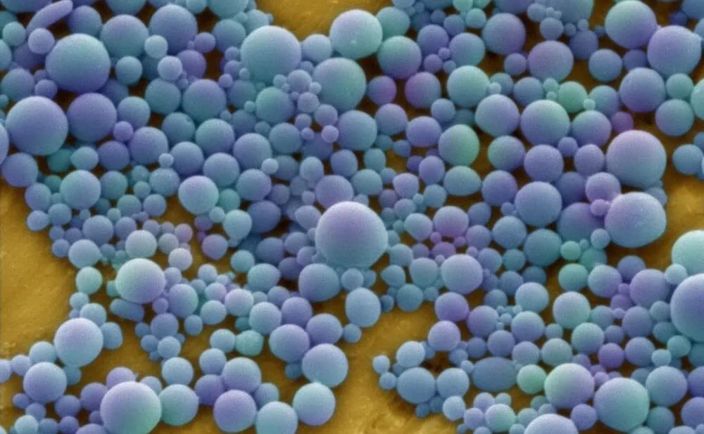
Microfluidics nanomaterial synthesis pack
Microfluidics for production of nanomaterials using sheath flow focusing
✓ Efficient synthesis. ofnanomaterials
✓ Easy microfluidic system implementation
✓ Biomedical applications
Lab-on-a-chip applications (e.g. nanomaterial synthesis)

Gut-on-a-chip pack
Intestinal cells coculture under flow, mimicking the gut physiology
✓ All microfluidic pieces included, quick and easy assembly
✓ Dynamic culture conditions
✓ Advanced in viro/ex vivo
Gut-on-chip
Applications requiring specific-chip design and chemical inertia
And many more!
Technical specifications
The polystyrene (PS) molding microfluidic setup comprises:
Heat press with double heating plate
| Components | Specifications |
|---|---|
| Dimensions | 420*550*680mm |
| Max temperature | 300 °C |
| Pressure range | 0-25 tons |
Laminator
| Components | Specifications |
|---|---|
| Dimensions | 270*545*130 mm (L x w x h) |
| Max laminated width | 335 mm |
| Max laminated thickness | 35 mm |
| Max temperature | 140 °C |
Options: Drilling machine
Consumables:Polystyrene sheets
Frequently asked questions
Does the process also involve mold fabrication?
Currently, the polystyrene (PS) molding microfluidic setup focuses on the chip fabrication and bonding from a pre-existing mold. However, we do have expertise to advise you in how to make your own molds.
What is the resolution of the Polycarbonate microfluidic devices?
Resolutions as low as 15 µm (channel width) for an aspect ratio of 2:1 can be achieved.
What maximum pressure can the devices withstand?
Based on internal testing, up to 3.5 bar.
What material can I use to close the chip?
The chip can be closed with a thermoplastic slide, a microscope glass slide or a microscopy-compatible polymer slide.
Is this process compatible with microscopy/reversed microscopy?
Polystyrene is optically transparent and well-adapted to microscopy.


Funding and Support
The BIOPROS and MICRO4NANO projects results helped develop this instrument pack, with funding from the European Union’s Horizon research and innovation program under HORIZON-CL4-2021-DIGITAL-EMERGING-01-27, grant agreement no. 101070120 and the European Union under H2020-MSCA-RISE-2020, grant agreement No. 101007804.
Products & Associated Accessories
FAQ - Polystyrene (PS) molding microfluidic setup
What is this PS molding system to replace (why would I even change away from PDMS?
It is intended as a viable alternative to traditional PDMS prototyping when PDMS becomes a hindrance: poor chemical compatibility, excessive gas permeability, and a throughput-insensitive workflow. The PS route retains the fast-cycle attitude, delivering a hard-polymer thermoplastic that behaves more like a finished-product material than an easy-to-work elastomer.
What is the actual speed of the PS chip fabrication process?
The time mentioned is approximately 1 hour to produce polystyrene chips, assuming you are using an existing mold and running the machine as planned (hot embossing, finishing, sealing). The promise of the pack is essentially that: you will get back to fast iterations without PDMS.
Special microfabrication infrastructure or cleanroom required?
No. The entire process is shown as taking place in an extravagant room. To a large number of European laboratories and alliances, that is no minor finick–it eliminates timing tension, access pressure, and a good deal of non-overt expense.
What are some of the differences in the process of the PDMS soft lithography?
PDMS typically includes mixing/degassing, pouring and curing, demolding, cutting, punching inlets, and bonding to glass using a plasma torch.
In the PS molding process, the MIC concept replaces the slow-curing step with hot embossing. After that, the chip is prepared using drilling tools and finally sealed with a plasma cleaner and a laminator. It is a sequence that can be done in the lab, only with optimization to be thermoplastic-friendly.
What about polystyrene in particular? Isn’t PS just “cheap plastic”?
PS is contextualized as a truly helpful microfluidic substrate: it is inert, rigid, biocompatible, and commercially feasible, production is cheap, and it is compatible with mass production. There are transparent grades that are important to observe under a microscope. In addition, the material is also said to be simple to shape into various shapes and sizes, so you are not confined to a particular geometry.
What resolution and features can I expect for channels?
Channel widths are cut to 15 μm, and an aspect ratio of 2:1 can be achieved. That is a practical point of reference for most lab-on-a-chip and cell-handling architectures, where robustness and reproducibility are at least as important as ever-smaller feature sizes.
What pressure can PS devices withstand in this methodology?
According to internal testing by MIC, the machines can withstand a pressure of 3.5 bar. When your application is pressure-sensitive (high transients, tight fittings, long routes), it is reasonable to treat it as proven value and to negotiate margins, sealing, and interconnect planning sooner.
What is the way you seal/close the polystyrene chip?
A thermoplastic slide, a microscope glass slide, or a microscopy-compatible polymer slide can be used to close the chip. In practice, this is what makes the workflow flexible: you can make the “window” (glass vs. polymer) either optics-friendly, thickness-friendly, or downstream-friendly.
What equipment is actually included in the setup (with concrete specification)?
The pack is basically constructed around two main machines plus optional drilling:
-Heat press with double heating plate
Dimensions: 420 x 550 x 680 mm
Max temperature: 300 °C
Pressure range: 0-25 tons
-Laminator
Dimensions: 270 x 545 x 130 mm (L x w x h)
Max laminated width: 335 mm
Max laminated thickness: 35 mm
Max temperature: 140 °C
Option: drilling machine
Consumables: sheets of polystyrene.
Mould fabrication in the package, or shall I turn up with a mold in my hand?
It currently specialises in chip fabrication and bonding on an existing mold. That said, MIC says they can guide you in creating your own molds, which is where projects usually waste time when switching from PDM to thermoplastics.