Optical detection techniques for microfluidics
Author
Alessandra Dellaquila, PhD
Publication Date
January 30, 2018
Keywords
Optical Detection
off-chip imaging
on-chip imaging
analytical biochemistry
electrochemical detection
Need advice for your optical detection techniques?
Your microfluidic SME partner for Horizon Europe
We take care of microfluidic engineering, work on valorization and optimize the proposal with you
Introduction to optical detection systems for microfluidics
Suitable detection techniques must be coupled to microfluidic technology to analyze experiment outcomes sensitively and scalablely. The most common methods are optical detection techniques, electrochemical detection, mechanical analysis, spectroscopy methods (Raman spectroscopy, NMR spectroscopy), and mass spectrometry (MS) [1-3].
This review represents a brief overview of the imaging-based detection techniques and systems for microfluidics and a final mention of the latest and most innovative methods.
Optical detection systems for microfluidics
Several classifications of optical detection techniques can be done based on the visual method, the imaging systems, or the presence or absence of lenses [3, 4]. Briefly, detection systems can be divided into off-chip (or free space systems) [5], in which detection components (light source, mirror, and detector) are not integrated within the microfluidic device, and light propagates in air and integrated (on-chip) devices [6, 7].
Optofluidic technology originates from the integration of micro-optics and microfluidics [8]. Lensless imaging can be performed through lens-free techniques [9, 10]. Furthermore, emerging imaging techniques use nanoparticle labels and nanoengineered materials for optical detection [4].
Conventional and off-chip imaging methods
The use of bulk systems such as microscopes and interferometers is still widespread. Thus, microfluidics have been widely coupled to bright-field, phase-contrast, confocal, DIC microscopy [2, 5], and interferometers [11]. Besides optical detection, chemical imaging can be performed using ATR-FTIR spectroscopy methods [12].
Visual detection is the dominant detection technique due to instrumentation availability and the ease of coupling the systems to microfluidic platforms [13]. However, these devices are difficult to miniaturize and show reduced sensitivity due to short optical path lengths [4].
Also, because of optics rapid development, optical detection uses LEDs, lasers, and diodes as light sources, microlenses, waveguides, and optical fibers for detection and PMTs, CCDs, and CMOS as sensors [7].
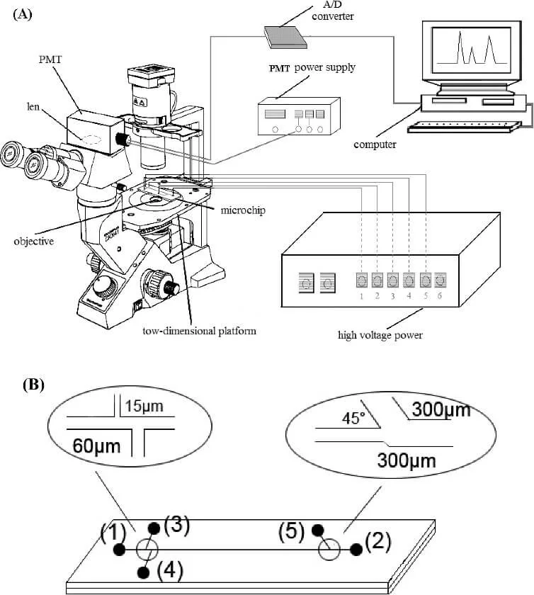
Integrated imaging methods (on-chip imaging)
In on-chip imaging systems, optical and optoelectronic components are fully integrated within the microfluidic platform [1]. The main advantages of these systems in comparison with off-chip devices are operator independence [6], increased portability, sensitivity, integration, and the ability to tune the optical properties [15]. Furthermore, on-chip imaging can be performed through lens-free techniques such as shadow imaging or digital inline holography [9, 16].
Download the MIC Horizon Europe 2026/2027 Calls Calendar:
Optical detection techniques for microfluidic applications
The following table reports the most common imaging techniques. Based on the analytes, these techniques can be used for detection in analytical biochemistry (detection of proteins, cytometry, enzyme kinetics), POC diagnostics, cell biology, immunoassays, as well as in screening applications and fluids manipulation [2, 13, 17]. Their application is not limited to the healthcare field but extends to industrial and environmental areas.
Table 1. List of the most diffused optical techniques, their operating principle and characteristics [4, 6, 7].
| Technique | Principle | Properties |
| Absorbance | Measure of the attenuation of incident radiation in function of the wavelength | Simple instrumentation Low sensitivity |
| Fluorescence | Measure of emission light from a fluorophore | High sensitivity High selectivity Ease of incorporation |
| LIF and LEDIF | Excitation is caused by a laser or LED source | Focus on small volumes and low reagents amounts Single molecule detection |
| Chemi- luminescence |
Measure of energy release in a chemical reaction | High sensitivity and portability Does not require a light source Limited number of reagents Poor reproducibility |
| SPR | Measure of refractive index change of a sample in contact with a metal film | High sensitivity Complex and expensive instrumentation |
| Interferometers-based techniques | Measure of the phase shift caused by the analyte binding | High sensitivity Label-free |
| SERS | Measure of plasmonic effect of metal substrates or nanoparticles | High reliability and reproducibility High sensitivity |
Optical detection components for microfluidics
Light sources
Commercial LEDs and miniaturized diode lasers as light sources have been widely used in microfluidics setups because of their availability and low cost. In contrast, in current literature, organic LEDs (OLEDs) and dye lasers are the most commonly used optofluidic light sources because they are easily fully integrated within microfluidic systems and their versatility [13].
Optical components to increase detection
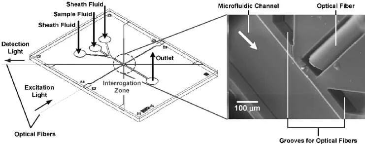
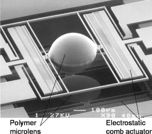
A standard and diffused approach uses optical fibers that can transmit and detect light, are easy to come by, and are suitable for combination with other optical components. Introducing microlenses and waveguides can improve absorbance, fluorescence, and interferometry measurements. Waveguides can be classified as transient wave-based, such as liquid-core waveguides (LCWs), or interference-based, as in the case of photonic crystal ARROWs detectors [6].
Detectors
Optical detection can be performed using a wide range of different detectors; conventional ones are PMT, and CCD sensors, where CCDs also allow multiplexing [4]. Integrated detectors are usually photodiodes (silicon or organic OPDs) and CMOS sensors that permit lens-free imaging.
New perspectives for optical detection systems in microfluidics
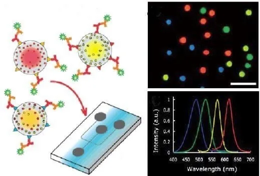
As the demand for cheap, automated, robust, and portable platforms for various applications increases [19], sensitive and scalable optical detectors are required. As described by Myers et al., a new class of imaging detectors can be identified in nano-engineered probes, such as quantum dots (QDs), nanoparticles, and biosensors [4].
Interestingly, the development of smartphone-based microfluidic platforms enables fast, low-cost, and straightforward analysis by using the smartphone camera as both a light source and detector [20]. Moreover, attempts have been made to develop platforms with imaging systems based on high-speed optical technology [21] and nanoscopy to go beyond conventional visual detection methods’ spatial and temporal limits.
Abbreviations: ARROW, antiresonant reflecting optical waveguides; CCD, charge-coupled device, CMOS, complementary metal-oxide-semiconductor; LCW, liquid-core waveguide; LED, light-emitting diode; LEDIF, LED-induce fluorescence LIF, laser-induced fluorescence; OPD, organic photodiode; PC, photonic crystal; PMT photomultiplier tube; POC, point-of-care; SERS, surface enhanced Raman spectroscopy; SPR surface plasmon resonance.
References
- K. B. Mogensen, H. Klank, and J. P. Kutter, “Recent developments in detection for microfluidic systems,” Electrophoresis, vol. 25, no. 21–22, pp. 3498–3512, 2004.
- Y. Zhu and Q. Fang, “Analytical detection techniques for droplet microfluidics-A review,” Anal. Chim. Acta, vol. 787, pp. 24–35, 2013.
- J. Wu and M. Gu, “Microfluidic sensing: state of the art fabrication and detection techniques,” J. Biomed. Opt., vol. 16, no. 8, p. 80901, 2011.
- F. B. Myers and L. P. Lee, “Innovations in optical microfluidic technologies for point-of-care diagnostics,” Lab Chip, vol. 8, no. 12, p. 2015, 2008.
- J. Wu, G. Zheng, and L. M. Lee, “Optical imaging techniques in microfluidics and their applications,” Lab Chip, vol. 12, no. 19, p. 3566, 2012.
- H. Gai, Y. Li, and E. S. Yeung, “Optical detection systems on microfluidic chips,” in Microfluidics, Springer, 2011, pp. 171–201.
- B. Kuswandi, Nuriman, J. Huskens, and W. Verboom, “Optical sensing systems for microfluidic devices: A review,” Anal. Chim. Acta, vol. 601, no. 2, pp. 141–155, 2007.
- X. Fan and I. M. White, “Optofluidic microsystems for chemical and biological analysis,” Nat. Photonics, vol. 5, no. 10, pp. 591–597, 2011.
- Z. Gorocs and A. Ozcan, “On-chip biomedical imaging,” IEEE Rev. Biomed. Eng., vol. 6, pp. 29–46, 2013.
- S. J. Moon, H. O. Keles, Y. G. Kim, D. Kuritzkes, and U. Demirci, “Lensless imaging for point-of-care testing,” Proc. 31st Annu. Int. Conf. IEEE Eng. Med. Biol. Soc. Eng. Futur. Biomed. EMBC 2009, vol. 24, pp. 6376–6379, 2009.
- Y.-C. Ahn, W. Jung, and Z. Chen, “Optical sectioning for microfluidics: secondary flow and mixing in a meandering microchannel,” Lab Chip, vol. 8, no. 1, pp. 125–133, 2008.
- K. L. A. Chan, S. Gulati, J. B. Edel, A. J. de Mello, and S. G. Kazarian, “Chemical imaging of microfluidic flows using ATR-FTIR spectroscopy,” Lab Chip, vol. 9, no. 20, p. 2909, 2009.
- H. Yang and M. A. M. Gijs, “Micro-optics for microfluidic analytical applications,” Chem. Soc. Rev., vol. 47, pp. 1391–1458, 2018.
- S. Zhao, X. Li, and Y.-M. Liu, “Integrated Microfluidic System with Chemiluminescence Detection for Single Cell Analysis after Intracellular Labeling,” Anal. Chem., vol. 81, no. 10, pp. 3873–3878, 2009.
- D. Psaltis, S. R. Quake, and C. Yang, “Developing optofluidic technology through the fusion of microfluidics and optics,” Nature, vol. 442, no. 7101, p. 381, 2006.
- M. Roy, G. Jin, D. Seo, M. H. Nam, and S. Seo, “A simple and low-cost device performing blood cell counting based on lens-free shadow imaging technique,” Sensors Actuators, B Chem., vol. 201, pp. 321–328, 2014.
- N. M. M. Pires, T. Dong, U. Hanke, and N. Hoivik, “Recent developments in optical detection technologies in lab-on-a-chip devices for biosensing applications,” Sensors (Switzerland), vol. 14, no. 8, pp. 15458–15479, 2014.
- S. Kwon and L. P. Lee, “Micromachined transmissive scanning confocal microscope,” Opt. Lett., vol. 29, no. 7, pp. 706–708, 2004.
- P. Abgrall and A. M. Gué, “Lab-on-chip technologies: Making a microfluidic network and coupling it into a complete microsystem – A review,” J. Micromechanics Microengineering, vol. 17, no. 5, 2007.
- S. C. Kim, U. M. Jalal, S. B. Im, S. Ko, and J. S. Shim, “A smartphone-based optical platform for colorimetric analysis of microfluidic device,” Sensors Actuators, B Chem., vol. 239, pp. 52–59, 2017.
- K. Goda et al., “High-throughput single-microparticle imaging flow analyzer,” Proc. Natl. Acad. Sci., vol. 109, no. 29, pp. 11630–11635, 2012.

Funding and Support
Review done thanks to the support of the DeLIVER H2020-MSCA-ITN-2017-Action
“Innovative Training Networks” – Grant agreement number: 766181
Author: Alessandra Dellaquila, PhD
Contact:
Partnership[at]microfluidic.fr

Check the other Reviews
FAQ - Optical detection techniques for microfluidics
Off-chip vs on-chip optics: what is the truth of the matter?
In off-chip (free-space) systems, the optical components remain external to the device, relying on microscope objectives, standalone light sources, mirrors, and external detectors. This approach is familiar, flexible, and easy to modify, making it well-suited for laboratory development and early experimentation.
On-chip optics, in contrast, integrate optical or optoelectronic elements directly into the platform itself, using waveguides, fibers, microlenses, or embedded sources and detectors. By bringing the optics into the device architecture, systems become more compact, robust, and portable. This integration reduces alignment complexity, enables greater operator independence, and opens a realistic path toward deployable, field-ready instruments.
Ultimately, off-chip solutions offer accessibility and versatility, while on-chip integration enables scalability and practical deployment. The choice depends on whether the goal is experimental flexibility or a self-contained, fieldable device.
What is the challenge with short optical path length (particularly with absorbance)?
Absorbance detection is conceptually simple: it measures light attenuation as a function of wavelength. In microfluidic systems, however, the microscopic dimensions of the channels inherently limit the optical path length. Because absorbance scales directly with path length, this reduction can significantly compromise sensitivity.
As a result, what appears straightforward in theory often becomes marginal in practice. Signals that look adequate on paper may prove too weak on a real chip unless the optics or geometry are deliberately redesigned, for example, through integrated waveguides, multipass configurations, or extended path-length channel designs.
This trade-off between miniaturization and sensitivity remains a key constraint in chip-scale absorbance detection, as highlighted in MIC’s technical assessments.
It appears that fluorescence is in charge. Is it merely a habit, or is it technologically better?
A bit of both. Fluorescence is sensitive and selective and is tolerant to small sample volumes. It is also consistent with what other labs already provide (fluorescent probes, immunoassays, cell staining). Laser-induced fluorescence (LIF) and LED-induced fluorescense (LEDIF) and you can scale down to extremely small interrogation volumes- in ideality down to single-molecule demonstrations. The compromise is to refer to chemistry, photobleaching thought, and (as per ambitions) optical complexity.
When chemiluminescence would beat fluorescence?
Chemiluminescence may be surprisingly appealing when it requires portability and simplicity: no excitation light source is needed and this eliminates an entire mass of optical equipment and alignment. It may be very delicate as well. However it is not magic, reagent options may be less free, reproducibility may be problematic and kinetics are important (your signal is born and dies along the reaction profile). This renders it to suit well to certain point-of-care style assays and not suit well to others.
Why bother with SPR and interferometer-based techniques when fluorescence is so good?
They are responding to another question: label-free detection. The change in the refractive index close to a metal film is traced by SPR, the change in phase due to binding or concentration is traced by interferometric techniques. Such techniques are quite delicate and delicate, particularly when the labels would perturb binding kinetics or when you desire actual biophysical measurements. The price is sensible complexity: optical stability, optical alignment, and usually even expensive instrumentation.
In what place does SERS come in, and why is it always referred to as having plasmonic substrates?
SERS (surface-enhanced Raman spectroscopy) uses plasmonic effects of metal nanostructures or nanoparticles in order to enhance Raman signals. It is the attraction of chemical specificity and strong sensitivity; the engineering fact is that to achieve reliable and reproducible improvement you have to regulate the plasmonic environment (substrates, nanoparticles, surface chemistry). When done well, it is a great between “imaging” and “molecular fingerprinting.”
What are the so-called lens-free techniques, and why are they important?
Lens-free imaging (shadow imaging, variants of inline holography) eliminates bulk optics and can make systems cheaper, thinner, and easier to ruggedize. You do not have the classical objective lenses but instead use computational reconstruction or geometric shadowing. This is very compelling, especially when the point-of-care or distributed testing is involved, and you would not wish to deliver a microscope. It would also be well-suited to microfluidics, as in microchannels, samples are confined to predictable planes and volumes.
Which elements become the most significant to me, in case I need to construct a real instrument?
Typically: (1) the type of light source (LEDs versus diode lasers; occasionally OLEDs or dye lasers when integration is the main goal), (2) the method of delivering/gathering light (free-space, fibers, waveguides), and (3) the type of detector (PMTs versus CCD/CMOS when imaging is required; readout can be scaled). This secret sauce is frequently in optical plumbing, fibers, microlenses, waveguides, and in minimizing the sensitivity to alignment, such that the device would be in week 1 and month 12.
What are liquid-core waveguides (LCWs) and ARROW structures?
LCWs direct light across a liquid core (which is useful to increase the length of interaction to enhance absorbance/ fluorescence). The ARROW-type structures (antiresonant reflecting optical waveguides) are structures that trap light in a manner that can be integrated on a chip scale (chip-scale integration) and detectable with high sensitivity (chip-scale sensitive detection).
What is the best way to select an optical method of detection to use in my application without over-engineering the system?
It can be an empirical approach to begin with three constraints, rather than the most imaginative method:
Typical range of analyte and expected concentration (and acceptance of labeling)?
Is it a requirement to have imaging (spatial information) or simply a quantitative signal?
Will it be the end target of a lab-prototype system, or a portable/robust system?
In most biochemical analyses, fluorescence or chemiluminescence has the least time to turbo. To have binding kinetics and label-free sensing, It may be worth the complexity to use SPR or interferometry. And should the north star be portability: lens-free paths or integrated optics are no longer a good idea, but the architectural choice.
In which projects of optical detection can the Microfluidics Innovation Center (MIC) contribute particularly in consortia of Horizon Europe?
MIC provides targeted support in the development of optofluidic and microfluidic systems, including prototyping strategy, microfabrication planning, and the design of testing setups with defined alignment and calibration specifications. Beyond the technical work, we also help structure proposals and shape valorization strategies, translating technical ambition into credible work packages, deliverables, and measurable impact.
Including a specialized microfluidics SME in a consortium can significantly strengthen a proposal. It brings greater clarity to risk management, a more coherent and practical integration plan, and a realistic pathway toward a functional demonstrator.