Microfluidics quantum technology: LasIonDef
Author
Christa Ivanova, PhD
Publication Date
September 14, 2020
Status
Keywords
Artificial Intelligence
quantum technology
3D printed microfluidic prototypes
photonic structures
electronics development
microfluidic device design
Your microfluidic SME partner for Horizon Europe
We take care of microfluidic engineering, work on valorization and optimize the proposal with you
Microfluidics quantum technology: introduction

Microfluidics quantum technology explained: The field of quantum photonics is significant for quantum communication technologies, requiring the transmission of quantum information since the transfer of single photons is fast and relatively free of decoherence.
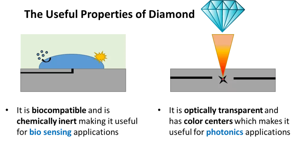
However, a truly scalable source of single photons is still an outstanding challenge. The controlled creation of deterministic single photon quantum emitters in comprehensive bandgap materials, such as the nitrogen-vacancy (NV) color center in diamonds and additional quantum emitters in diamonds and other materials, is therefore essential for practical quantum technologies.
Novel sensing devices based on the NV centers’ spin, which has unparalleled room temperature coherence, offer quantum-enabled magnetic, electric, and biosensing with unprecedented sensitivity. Microfluidics quantum technology opens the way to lab-on-a-chip devices enabled with quantum sensing capabilities (Nano Lett., 2015, 15(3), 1481).
The effort to harness ‘spooky’ quantum phenomena such as entanglement, which can be observed in laboratory conditions, into practical technologies will require the development of new techniques in high-performance material systems that can allow the generation, protection, manipulation, and measurement of single photons by quantum emitters, and the integration of these quantum emitters with photonic and microfluidic structures.
Microfluidics quantum technology: project description
The LasIonDef consortium researchers work to boost all the necessary technical and scientific advances to develop the next-generation microfluidic quantum technology.
Our efforts are focused on the creation of 3D printed microfluidic prototypes, fluidic interfacing, and post-fabrication characterization of diamond microchannels and devices, as well as on the development of novel microfluidic instrumentation and artificial neural network models for the characterization of the channels and their fabrication.
Juan Sandubete will be working on the software portions of the project, including electronics programming, simulation and model development, software interfaces, and artificial intelligence tools for microfluidic quantum technology. He is enrolled at the doctoral school of The Universidad Complutense de Madrid under the academic co-supervision of Prof. José Torrecilla.
Bibek Raut will focus on the project’s hardware sections, including mechanical components and microfluidic device design, 3D printing, and electronics development. He is enrolled at the ED3C doctoral school of the Université de Sorbonne under the academic co-supervision of Prof. Patrick Michel of the Paris Brain Institute (ICM).
Related content
In the light of this project, we have published two reviews: one about the microfluidic technological revolution and innovative applications and the second about materials and fabrication techniques of microfluidic chips.
Funding
This project has received funding from the European Union’s Horizon research and innovation program under the Marie Skłodowska-Curie grant agreement No 956387 (LasIonDef).
Start date: 01 Oct 2020
End date: 20 Sept 2024
Researchers
Juan Sandubete
Marie-Curie PhD candidate Elvesys/Universidad Complutense de Madrid
- Electronics, Robotics and Mechatronics degree by the Univerisad de Sevilla (B.Sc.)
- Systems and Control Engineering by the Universidad Complutense de Madrid (M.Sc.)
Areas of expertise:
Robotics, advanced automatic control techniques, electronics, embedded systems programming, artificial intelligence, and signal processing.

Bibek Raut
Marie-Curie PhD candidate Elvesys/Sorbonne Université
- Bioengineering and Robotics, Tohoku University, Japan (B.Sc.)
- Fine mechanics, Tohoku University, Sendai, Japan (M.Sc.)
Areas of expertise:
Additive manufacturing, 3D CAD design, tissue engineering, bio sensing, electronics.

![]()

Check our Projects
FAQ – Microfluidics quantum technology: LasIonDef
What was LasIonDef apparently trying to resolve?
In quantum photonics, we require high-quality single-photon sources to carry quantum information with minimal decoherence. It is still the bottleneck today. LasIonDef embarked on the design and characterization of microfluidic-photonic devices, particularly diamond microchannels containing quantum emitters such as nitrogen-vacancy (NV) centers, to transform clever lab demonstrations into repeatable, scalable devices.
What in quantum tech can microfluidics be useful in?
Microfluidics makes it possible to have tight control of the environment – flow, temperature, and chemical composition around the emitter. That is, charge states can be tuned, surface chemistry controlled, and emission stabilized. Also, this enables lab-on-chip quantum sensing: a sample is passed through a channel, and quantum signals are measured locally rather than moving the sample to large instruments.
What was the technical contribution that the MIC team created?
Three pillars:
- Fast 3D-printable, replicable microfluidic models plus tough fluidic interfacing of diamond devices.
- The fabrication of diamond microchannels and the characterization of emitter-photonics coupling were done post-factum.
- Electronics, simulations, and neural-network models as new instrumentation and software to accelerate channel characterization and feedback fabrication.
Who did what on the project?
Two Marie Curie PhD students led two streams. Juan Sandubete was a programmer, software engineer, modeler, interface designer, and AI tool. The work of Bibek Raut was grounded in hardware and mechanical design, microfluidics, additive manufacturing, and embedded electronics. The two had equal supervision in European doctoral schools to maintain academic rigour and industry relevance.
What would you want to purchase using AI-assisted characterization that you can not purchase using standard metrology?
Speed and consistency. Optimizing neural models for optical/microfluidic measurements can be used to classify channel quality and predict the fabrication modifications needed to achieve target geometries or regimes. That completes the process of design and creating without weeks of trial and error.
Does it have any publications that put the state of the art into perspective?
Yes, there will be two domain reviews, both based on this project: one on the technological revolution in microfluidics and its new uses, and one on the new materials and fabrication methods in microfluidic chips. These present the bigger picture and the materials playbook for the prototypes created herein.
Are you developing a quantum sensing or photonics consortium? In that case, what is the role of MIC?
MIC generally assumes microfluidic engineering (design, rapid prototyping, interfacing), instrumentation and automation, as well as proposal valorization (work package design, exploitation planning). Within the context of our experience with several EU consortia, the context has enhanced the credibility of implementation and exploitation through the insertion of a specialized SME. We have a successful track record of consortia such as MIC increasing their proposal success rates by approximately 2x the official average – the reviewers are convinced that there is a viable way to go from a prototype to a product.
What would the initial collaboration step entail?
Two rapid prototypes: (i) a scoping sprint (2-4 weeks) to represent your quantum use case into microfluidic architecture, risk table, and TRL roadmap; (ii) a prototype loop, in which emitter control and fluidic conditions are coupled, and whose characterization is aided by AI. Based on that, we assist in strengthening the design for submission to Horizon Europe or for direct tech transfer.
Any real limitations or restrictions of interest?
Yes. The issue of uniformity in single-photon emissions still requires emitter stat, surface chemistry, and diamond processing, which may introduce defects at the quantum scale. Microfluidic packaging must withstand optical power, thermal loads, and wet operating conditions. The idea behind the LasIonDef approach is to put these variables in place and testable long before you have spent months of your life trying to test a dead-end geometry.
Which applications are the closest to being deployed?
The near-future sweet spot: biosensing, magnetometry, and label-free quantum sensing within microchannels. Room-temperature quantum sensing – the near-term quantum sweet spot – biosensing, magnetometry, and label-free quantum sensing within microchannels. The more challenging case of deterministic single-photon communication sources is of interest; however, the same platform also helps standardize testing and facilitates materials learning cycles.
What is scalable in this context?
Scalability refers to the consistent performance of devices across repetitive tasks, standardized tests, and interface protocols. Fabrication of diamond at the wafer scale is on the rise, though LasIonDef has focused on fixtures, 3D-printed microfluidics, and software/hardware stacks that allow other labs to replicate their work without purchasing special tooling. It provides the foundations for future wafer-scale implementation.
Am I out of quantum? Is this transferred to classical photonics or bioanalytics?
Quite a bit. The identical microfluidic design, expeditious prototyping, and AI-driven quality management enable photonic biosensors, micro-opto-fluidic assessments, and fine-tuned flow direction for sensitive emitters or detectors. The patterns are transferred, in case you happen to be transporting photons and fluids in constrained spaces.